

Thermo Fisher Scientific Rolls Out Helios G4 SEM
Helios G4 plasma-focused dual ion beam (FIB) system is designed to de-process and provide ultra-high-resolution scanning electron microscope (SEM) analysis on semiconductor devices.
Can perform failure analysis applications from high-speed delayering to SEM cross-section imaging of devices and TEM sample preparation. Used to expose metallization layers, permitting electrical fault isolation and analysis with nanoprobing tools. Can support de-processing down to 7nm node and offers automated end pointing that stops milling automatically when the metal or via layer of interest is exposed. Reportedly provides up to 10 to 20 times faster milling rates than conventional (Ga+) FIB solutions, permitting larger samples for nanoprobing and TEM imaging, as well as large-area SEM cross-sections, on a range of advanced (2.5D) packaging, LED, display and MEMS.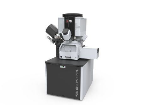
Thermo Fisher Scientific
thermofisher.com
Register now for PCB West the Silicon Valley's largest PCB industry trade show: pcbwest.com!


Press Releases
- IDTechEx Report Unveils 3D Electronics Status and Opportunities
- Hon Hai Technology Group (Foxconn) Pledges 100% Renewable Electricity By 2040 and Joins RE100
- ZESTRON Academy Introduces Cutting-Edge SMT Webinar Series for 2024
- AIM to Highlight NC259FPA Ultrafine No Clean Solder Paste at SMTA Juarez Expo & Tech Forum