

Current Issue
Embedded Passive Technology Materials, Design and Process
A summary of resistor material selection, evaluations and duplication of a complex digital design.
The concept behind embedded passives technology (EPT) is to fabricate and bury components such as resistors and capacitors (R&C) within the layers of a substrate during its fabrication.1 EPT drivers include demand for additional functionality at the same or lower price, better electrical performance, higher packaging density and technologies with potential cost savings. Using EPT, passive components may be embedded into the substrate directly under active devices such as ASICs. The shorter distance between the embedded passives and active components reduces parasitic losses associated with surface-mounted passives, resulting in better signal transmission and less crosstalk. Lower loss and lower noise yield an improvement in electrical signal performance, especially at high frequencies. Passive components account for 80 to 95% of the total number of components and cover over 40% of the surface of the PCB.
Reducing the number of surface mount passives will increase available real estate and therefore permit higher packaging densities. It has the potential to reduce material costs due to fewer purchased components and manufacturing materials (flux and solder), lower defect per million opportunities (DPMO), improve yield, and reduce production cycle time and time to market, as well as reduce cost of poor quality (COPQ). EPT can simplify assembly and test processes and reduce the actual cost, especially when using 0201 packages or lead-free processes. EPT reduces overall product cost in comparison with traditional use of discrete SMT components.
The Honeywell Advanced Manufacturing Engineering technology group has evaluated embedded passive technology as part of the Game Changers technology roadmap. The game changer of EPT was defined in three different phases. Phase 0, completed in 2009, defined the type of resistive materials available. Phase 1, completed in 2010, selected resistive material types, and designed, assembled and tested a test vehicle under the following conditions: ESD, non-ESD, IST coupon testing, thermal testing at -55° to 125°C and lifecycle and mechanical vibration and displacement test. Phase 2 is in the final phases of completion, where a high-complexity circuit card assembly (CCA) was selected using Thermount-based material for board fabrication with four layers of EPT (Ticer resist materials 25Ω and 1kΩ, and 3M C-Ply) embedded materials, in a 20-layer stackup with multiple impedance control layers.
Design and functionality. Customer demands for increased functionality for aerospace applications have resulted in high-density PCB designs that are low yield and high complexity, DfM violations, and significant hidden factory rework during assembly. EPT provides a means to reduce the number of surface-mounted components, thus increasing yields and freeing real estate (FIGURE 1). Although capacitors, resistors and inductors are all candidates for embedding, most current interests focus on capacitors and resistors since they represent the majority of passives used on a board. A generic single board is generally composed of 5% integrated circuits (ASICs), 4% connectors, 40% capacitors, 33% resistors and 18% miscellaneous parts.2 Embedded resistors and capacitors can be individually fabricated, and capacitors can also be manufactured in distributed planar form.
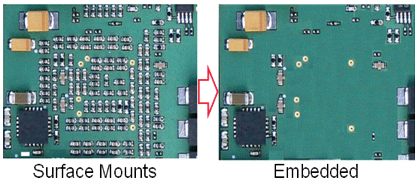
Figure 1 . Surface mount assembly vs. embedded technology.
One concern about EPT is whether the technology is economically feasible. Advantages of EPT are the possibility to reduce assembly costs, negate the cost of purchasing and handling discrete passive components, and reduce required board size area. However, these advantages must be considered against the increased cost of board fabrication and decreases in throughput and yield of the board fabrication process.
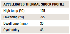
Embedded material tests. The resistive material benchmark Ticer thin film resistor foil is thermally and electrically stable after thermal cycles. Lifecycle thermal testing was conducted using TABLE 1 parameters for 300 cycles per IPC-6012 class 3 accelerated thermal shock profile. This is the profile used to qualify all Honeywell AERO FR-4 board materials and represents 20 years’ life reliability of the product.
Table 1. Thermal Profile for Accelerated Qualification Test
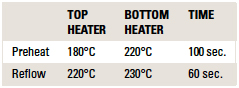
BGA rework was performed on the multiple substrates where BGAs were removed and replaced using an SRT Model 1100 repair and rework station under the normal removal and replacement thermal profile. TABLE 2 defines thermal parameters for removal and replacement.
Table 2. Removal and Replacement Thermal Profile
ESD testing was conducted using two different lots: one with best-in-class ESD protection and the other without ESD protection. The ESD test concluded that there is no difference in resistance percentage change between the ESD and non-ESD (FIGURE 2) controlled boards during the assembly.
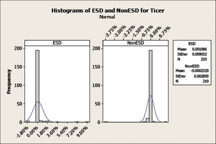
Figure 2. No difference between ESD and non ESD.
Ticer materials also provide excellent thermal stability. NiCr, Nickel Chromium Aluminum Silicon (NCAS), and Chromium Silicon Monoxide (CrSiO) are well known for their excellent thermal stability under continuous load and thermal excursion. The materials can be subjected to multiple thermal excursions, such as lead-free (RoHs) reflow, with minimal resistance change and ensured long-term reliability.
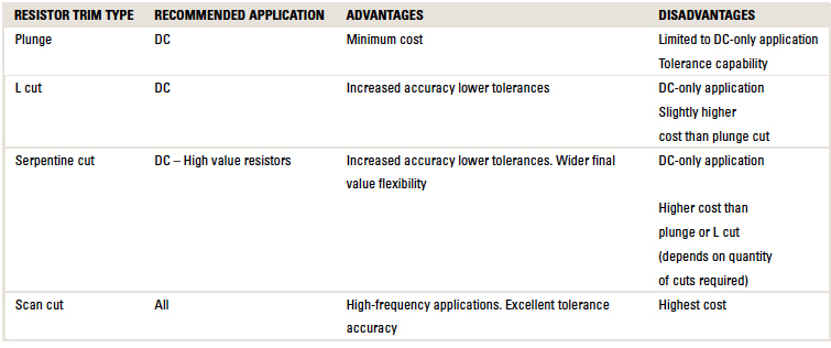
Material specifications. TCR integrated thin-film resistor foil is supplied in a variety of widths and thicknesses using grade 3 copper foil. The thicknesses of 18µm (0.5oz.) and 35µm (1oz.) are commonly available. TABLE 33 shows materials specialization and recommended etching solutions.
Table 3. Resistor Trim Types Advantages and Disadvantages
Design. Design for the EPT components’ shape is based on final resistor required value and embedded resistance material value. The thin-film embedded resistor is isotropic; therefore, the resistor patterns can be designed in any orientation required by the I/O or to optimize spacing. The basic equation for calculating resistance is:
R = s(L/W) (Eq. 1)
where
R = resistance in ohms
s = sheet resistance in ohms/square
L = length of resistor
W = width of resistor
Note: the term “square” is dimensionless.
The final resistance tolerance is a function of the etch precision of the copper etch processes of the fabricator and resistivity variation of embedded film. To minimize the impact of etching on resistor tolerance, a fixed resistor width is recommended, with the resistor length adjusted to achieve the correct resistor value.
Another technique to improve resistor tolerance is to use larger dimensions since the line-width variation of the copper etch process is typically fixed and therefore independent of line-width. Designing with resistor widths and lengths greater than 0.25mm (0.010") is recommended. Consult the Honeywell AME resistor calculator model4 for determining recommended sizes based on tolerance and power dissipation.
Thermal and mechanical spacing allowances at plated-through and microvia holes can be challenging. A minimum of 0.25mm (0.010") is recommended for copper connection between the hole and the beginning of the resistor pattern. This ensures adequate isolation from the stresses caused by assembly soldering and hole drilling (FIGURE 3).
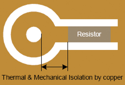
Figure 3. Resistor in ground plane.
Design for power and thermal dissipation is a function of the resistor alloy power rating (mW/mil²) and the resistor area (mil²). When higher power loading is required, the resistor must be sized accordingly. Factors that affect thermal dissipation are:
- Circuit configuration.
- Circuit thickness and material type.
- Thermal conductivity of the dielectric.
- Proximity of power or ground planes to resistor.
- Ambient temperature.
- Additional system cooling or heat sinking.
- Resistor size (total resistor area).
All aspects of the system’s thermal dissipation must be considered in the board design. Critical thermal dissipation requirements may require thermal profile modeling or actual prototypes to ensure proper configuration is achieved.
Design – resistor types. Designing for EPT resistor types can be determined based on the resistor value and electrical functionality. Two types of resistors can be used in embedded: resistors in very basic circuits, such as pull-up and pull-down, and precision resistors.
Pull-up and pull-down resistors are used in electronic logic circuits to ensure that inputs to logic systems settle at expected logic levels. FIGURE 4 shows a simple EPT design for pull-up and pull-down resistors. The typical value for pull-up/down resistors can vary in value; it ranges from 500Ω to 10kΩ, depending on the circuit logic. The typical tolerance of these resistor types can be up to 20%.
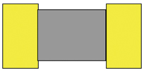
Figure 4. Rectangular configuration.
EPT precision resistors are characterized by a resistance value with a tolerance as low as 1%. To achieve the required precision tolerance of 1%, laser trimming method is applied.
Fabrication. Fabrication of PCBs with EPT involves the same processes as traditional fabrication, whereby embedded resistive materials are used as part of the stack-up structure. The NiCr resistor alloy reduces fabrication steps by eliminating the need for a separate resistive layer etch. NiCr can be etched first in cupric chloride, followed by ammoniacal etchant, the same etchant used to etch copper layers of the board. Also, use of double-treat copper can eliminate the need for laminate precleaners and oxide treatments. Board integrity is determined by traditional final testing, such as continuity, isolation and value measurements.
Several key fab processes (FIGURE 5) must be in control and possibly modified to ensure properly defined resistor patterns. These processes can be properly controlled, provided attention is paid to several considerations. Some considerations are the equipment setup for the photoresist application and subsequent exposure and development, and process control for selective copper removal to define resistor length, which can impact the value and tolerance.
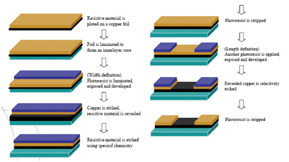
Figure 5. Illustration of EPT fabrication process.
Laser trimming. Rules for the laser trimming5 process require that circuits be square or rectangular and consist of straight lines, arcs, or a combination thereof. The resistor “length” is always the dimension of the resistor in parallel to the current flow. And the resistor “square” in the corner area(s) of a bent style resistor, such as “L” shape or serpentine design, should be counted as one-half the value of the sheet resistance (FIGURE 6). This can be demonstrated in the following equation:
R = S*(Sum (Square)+Sum(Corner)/2) (Eq. 2)
where
R = resistance in ohms
S = sheet resistance in ohms/square
Square = number of squares
Corner = number of right corners
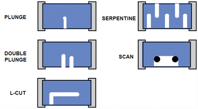
Figure 6. Illustration of resistor “square” basic calculation.
Based on design complexity, precision embedded resistors can be used and laser trimming is utilized. Laser trimming can achieve a tolerance of 1% utilizing several trimming methods, such as plunge, double plunge, L cut, serpentine and scan (FIGURE 7). Advantages and disadvantages of resistor trimming types are demonstrated in Table 3.
Figure 7. Illustration of laser trimming type.
Designing for laser trimming can be challenging and requires design for manufacturing and test. Configuration for resistor types can be designed in a variety of shapes. The resistor shape will determine the method of trimming. The resistor types are:
- Rectangular configuration. The most common type of resistor (Figure 6).
- L-bent configuration. This resistor “square” in the corner area of a bent style resistor should be counted as one-half the value of the sheet resistance (FIGURE 8).
- Serpentine configuration. This resistor is typically used for high value resistors. The number of corners complicates calculation of the value. The resistor “square” in corner areas of a serpentine style resistor should be counted as one-half the value of the sheet resistance (FIGURE 9).
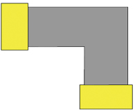
Figure 8. L-bent configuration.
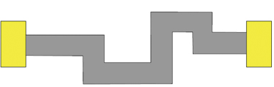
Figure 9. Serpentine configuration.
Top-hat (lobe type) configuration. The advantage of the top hat design is its wide trim range. FIGURE 10 shows a five square resistor. By trimming a single plunge cut of the laser, a nine square resistor can be created. The resistance can be manipulated between these values by limiting the amount of trim. Resistor with a trimmable range of more than three times the initial value can be created using this technique. This type of resistor must be trimmed, regardless of the tolerance requirement (FIGURE 11).
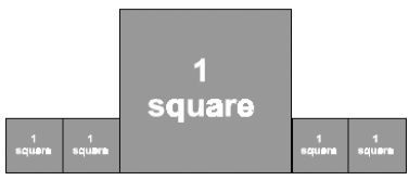
Figure 10. Top hat configuration.
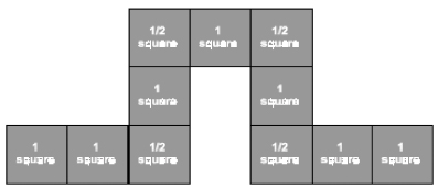
Figure. 11. Top hat configuration after plunge cut.
Tooling and trimming guidelines and requirements. Probe cards are required to measure all resistors as they are laser trimmed. It is best to design a probe card to measure 15 to 20 resistors at a time. Multiple cards would be required for designs that use more trimmed resistors. This will affect the circuit, tooling and setup pricing. Resistors with values of 50Ω or less require Kelvin-style, 4-point probing to ensure accuracy. The quantity of probe cards can be reduced by utilization of DfM modeling and determining the resistor’s unique values, shapes, and geometrical positioning.
The laser (Yag) spot is approximately 35-40µm diameter depending on the subject materials. This can be reduced to ~25µm with new optics. High accuracy trims (tolerance +/-0.5%) are best obtained for resistors larger than 0.020 x 0.020 in² (250 x 250µm) and are trimmable, depending on material and resistance values.
Some design considerations for precision resistors are:
- Thermal effect during laser trimming.
- Electrical current and potential during test and trim.
- Thermal coefficient of resistance may significantly reduce throughput performance and final process tolerances.
- Power and potential coefficient of resistance may significantly reduce throughput performance and final process tolerances.
- CAD data can be used in planning and programming the process before actual parts are available.
- Final resistor tolerance may be affected by after-trim board fabrication processes.
Power handling capability. The power handling capability of a thin-film embedded resistor is a thermal management issue in which the power handling capability is a function of the resistor’s size and shape, and the PCB construction. It is the relatively low degradation temperature of organics that makes thermal management important. The steady state heat transfer conduction through board is determined by
Q = k A1 (Tr –Ts) / d (Eq. 3)
And the steady state heat transfer convection from board by
Q = U A2 (Ts – To) (Eq. 4)
where
Q = heat in watts
Tr = resistor temperature
K = thermal conductivity
A1 = resistor area
A2 = board area
U = heat transfer coefficient
Ts = surface temperature at outer layer
To = environmental temperature
To avoid resistor failure
Tr < Tmp of resistor material (e.g., NiCr ~ 1400°C)
Tr < Tg surrounding organics (e.g., FR-4 ~170°C)
Tmp = temperature melting point
Tg = glass transition temperature
Power dissipation of thin film resistors. To understand the effect of resistor size on power dissipation,6 experiments have been done on thin-film resistors to measure the burnout power and the resistance change of thin film resistors under different power loads. The experiment resulted in the following:
Pb = Ib ² R / A (Eq. 5)
where
Pb = burnout power
Ib = burnout current
R = resistance
A = area of the resistor
The burnout current versus resistor size is plotted in FIGURE 12. It shows that the thermal dissipation ability of a thin-film resistor depends on the width and length, and on the size of the resistor. The narrower the width and the shorter the length, the higher the burnout power density because of the shorter heat conduction path to the surroundings. As resistor size increases, the burnout power density drops, although the total power increases because of the larger resistor physical size, indicating that the relationship between the total power dissipation and the thin-film resistor size is not linear. It was determined that the resistor should be operated at a power level of no more than 30 to 40% of the burnout power value to keep the resistor temperature low with no significant change in resistance.
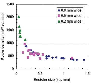
Figure 12. Burnout power of thin film NiCr resistor.
The resistance change of thin-film resistor under different power loads shows that, as power load increased, the temperature of the thin-film resistor increased, which in turn caused the resistance to change. The resistance change at different power densities calculated from the current load and the size of the resistor is shown in FIGURE 13 and FIGURE 14. Both NiCr and nickel-chromium-aluminum-silicate (NiCrAlSi) resistor materials were evaluated. For Figure 13, the resistance change is due to power load and the resulting temperature change and is a function of material TCR; this resistance change is reversible upon cooling of the resistor.
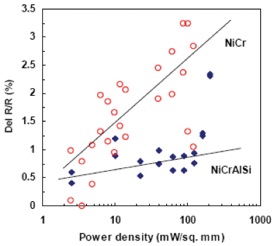
Figure 13. Resistance changes under power load, resistive foil was laminated on single side of FR-4 prepreg and the resistor size is 30 x 30 mil.
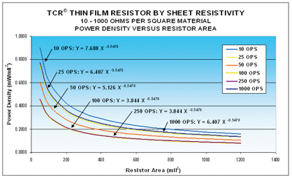
Figure 14. Power density vs. resistor area.
Resistor area calculation. The resistor value using embedded thin-film resistance is calculated by sheet resistance in ohms/square times the length to width ratio of the film – the “number of squares.”
R = (ρ/t) (L/W) = Rs Ns (Eq. 6)
where
R = resistance in Ω
Rs = ρ/t = sheet resistance, Ω/square
L and W = length and width of the material strip
Ns = L/W = the number of square
The following is an example using the Ticer Resistor Calculator to determine the size of the resistor based on the following parameters:
Problem. Resistor value needed is 100Ω; power needed is 200 mW, and thin film foil used is 25Ω/square.
Solution. To achieve the 100Ω value, the design requires 4 square of the Ω.
Power formula for the 25Ω/sq is defined as
p (mw/mil²) = 6.407 A (mil²) -0.5478 (Figure 14) (Eq. 7)
where
p = power density
A = resistor area
Calculating for A (Eq. 8)
P = p A = 6.407 A-0.5478 A = 6.407A 1-0.5478 = 6.407 A0.4522
A = (P/6.407) 1/0.4522
A = (200/6.407) 1/0.4522 = 2016.9 mil²
Calculation of resistor width and length is determined by
A = w (w x n) (Eq. 9)
where
w = resistor width
n = number of the squares
w = (A / n) 0.5
w = (2016.9 / 4) 0.5 = 22.45 mil
l = n w = 22.45 x 4 = 89.9 mil
The Ticer calculator provides guidelines to determine resistor size based on variables such as resistor value, power dissipation, tolerance and etch tolerance. It also provides resistor pattern shapes to optimize the footprint based on sheet resistivity. This calculator is located on the AME website.
Summary
Embedded passive technology is viable and has been reliably used in the defense and aerospace industry for over 20 years. EPT’s value is creating space on a crowded PCB where more active components are needed. Embedding resistors and capacitors can increase board functionality without increasing board size. It improves signal performance and reduces parasitics and crosstalk. EPT can increase reliability by eliminating surface mount devices and the defects associated with assembly processes such as placement and soldering.
Acknowledgments
The author extends his appreciation to John Garone, VP – VPD; Dave Dunn, VP – AME; Dr. Al Sanders, director, program engineering; Dr. John Klein, engineer fellow, and Hector Valladares, engineer fellow. Also, special thanks to Dr. Jiangtao Wang and Dave Burgess of Ticer Technologies for continued technical support.
Ed.: This paper was first published at SMTA International in October 2014 and is reprinted here with permission of the author.
References
1. R. Ulrich and L. Schaper, ed., Integrated Passive Component Technology, Wiley-IEEE Press, 2003.
2. L. Marcanti, and J. Dougherty, “Embedded Passives: Promising Improved Performance,” CIRCUITS ASSEMBLY, July 2001.
3. Ticer Technologies, Next Generation Integrated Thin Film Resistor, company literature.
4. TCR resistor calculator – ATP Applied thin-Film Products.
5. Laser resistor trimming design rules.
6. J. Wang, M. Davis, R. Hilburn and S. Clouser, “Power Dissipation of Embedded Resistors,” IPC Printed Circuits Expo, March 2003.
is AME Electronics Processing and Fabrication Technology Fellow at Honeywell Aerospace (honeywell.com); hikmat.chammas@honeywell.com.


Press Releases
- AIM Solder’s Dillon Zhu to Present on Ultraminiature Soldering at SMTA China East
- Hentec/RPS Publishes an Essential Guide to Selective Soldering Processing Tech Paper
- ZESTRON Welcomes Whitlock Associates as New Addition to their Existing Rep Team in Florida
- ROCKA to Showcase Expanded Services and Top Distribution Brands at Three SMTA Expos in May