

Current Issue
Creative Technological Solutions for Complex PCBs
What the optimal assembly solution for a 2-mil thick flexible PCB is, and other mysteries.
“Every problem has a solution; otherwise, there wouldn’t be a problem.”
The high-tech field requires capacity for creative thinking. Small form factors and thinner products lead to tiny components with smaller solder pads and tighter spacings. The interdependency of PCBs, materials and production processes requires an in-depth analysis during the planning and design stage of the soldering process and any potential failure points. Designers and manufacturers of these products must work in close cooperation, with the aim to find creative solutions, not to mention effective ones. Development engineers must plan and design product that will fully meet customer requirements, but no less important will be able to be manufactured efficiently and effectively.
We were approached by a company that manufactures a revolutionary product, a wireless microchip that tracks daily health conditions of patients who have had heart failures. The 10 x 1.2mm-sized PCB that constituted the core of the product encompassed several interesting technological challenges: 01005 (0.4 x 0.2mm) components, a component within a µBGA package, where the distance between leads (pitch) is 16 mil (0.04mm), and, as noted, a 2 mil (0.05mm) thick flexible PCB.
Upon analysis, it wasn’t difficult to determine the significant hurdle was the PCB thickness. A standard PCB is 1.6mm thick – some 320 times thicker than the PCB we were asked to assemble – and the machinery on the production line is able to handle thicknesses down to half that, or 0.8mm. A thinner PCB requires a platform on which the board will be seated during its transition through the production line. Given the board was very small as well, it was necessary to plan and design a panel with several PCBs and ensure during panel design it was possible to attach it accurately to the device.
The next hurdle was the component size. These components have very small (6 mil) solder pads, and it was essential to verify the pads receive the optimal amount of solder required for complete soldering. A thin (2.5 mil) stencil would permit application of an accurate yet minimal amount of solder paste. However, a stencil this thin is not rigid enough and can cause distortions during the stretching process performed by the printer. Therefore, we instead chose a step stencil that is 2.5 mils thick in the component areas but 4 mils thick on its edges in order to add mechanical strength to the mask during the spreading process.
Soldering the world’s smallest active component. In another instance, we built assemblies for an Israeli high-tech company that developed an electronic retina. The product constitutes a dream come true for millions of blind people worldwide. The company’s engineers have successfully traversed the complexity of the development of this innovative product that encountered considerable difficulties in production.
The product is based on a minuscule electronic component with an 11 mil (0.275mm) pitch between leads. It is the smallest active electronic component ever assembled on an SMT line as of today. Production at the time involved no fewer than four different suppliers to ensure optimal soldering of the component: the component manufacturer; the solder ball supplier; the PCB manufacturer; and the component assembler. The process was cumbersome, expensive and lasted eight weeks.
After some brainstorming, it was concluded the component could be assembled through a standard production process using several creative actions. It was decided to manufacture the PCB without solder mask (bridges) between the pads, and to assemble the component as is (without the addition of balls) in a typical placement process. In light of the accuracy required, the conductor was not covered by a solder mask during PCB production but rather remained exposed. In the first placement experiment performed, it was revealed the component’s pads lacked solder. Under analysis, it was realized the exposed conductor, due to surface forces, “stole” the solder from the pad. Taking this into consideration, a larger aperture was opened in the solder mask during the second experiment. In this manner, the new aperture covered both the pad and part of the conductor, in order to permit a larger volume of solder, thus enabling optimal soldering (FIGURE 1). The results of the second experiment (FIGURE 2) indeed showed the solder material fully covered the pad, and proper soldering was performed.
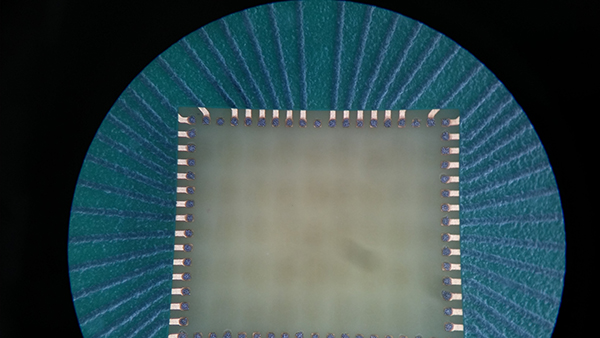
Figure 1. Shown are 6x6 mil pads, with 11 mils distance between pads, after printing and before soldering.
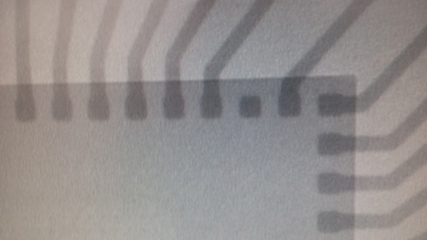
Figure 2. Shown are 6x6 mil pads, with 11 mils distance between pads, after soldering.
The advantages of the process were clear and explicit: The process is about 50% cheaper, the supply and delivery time about 70% shorter, and the soldering results are optimal.
Assembling a 1.4x14mm-sized micro PCB? Another interesting company wanted to assemble a 1.4x14mm-sized micro PCB. A PCB of these sizes cannot be assembled on an automated production line.
In this case, we designed a rectangular quadrilateral panel able to contain several PCBs in order to permit assembly on an automated line. The production line’s machinery comprises conveyor belts on which the PCBs are transported during the work process. The panel must be rectangular and quadrilateral to ensure stable movement on the belts. The panel design permits use of a generic PCB size, as well as optimal utilization of the production line. Using this method, the panel will be installed on the line and afterward the PCBs dismantled from it and transferred for further work.
The PCB area within the panel was significantly smaller than the area of an empty panel. Thus, copper cubes (copper balance) were defined within the vacant areas to ensure thermal balance during reflow and, likewise, to give the panel mechanical strength and stability. In addition, local fiducials were added beside every PCB for added precision during placement (FIGURE 3).
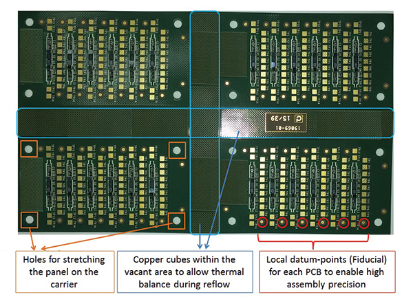
Figure 3. A 4x14mm micro-PCB on a panel.
The panel, which contained 24 PCBs, was attached to a rigid carrier (rack) throughout the placement process. The panel was firmly attached to the carrier by means of dedicated holes on the panel, which were used for stretching the panel on the carrier.
When PCBs become more dense and condensed, product development must take into account the PCB manufacturing considerations and concerns and integrate the designer and manufacturer in order to ensure the production process is feasible, efficient and qualitative. For their part, the PCB designer and manufacturer, who are usually subject to strict production rules, must be willing to think outside the box to determine how to match the development engineer’s requirements to the production capabilities. Even if the development requirement seems impossible for the production conditions, it is necessary to think creatively how to “square the circle” and suit it to the production floor.
is chief marketing and business development officer at Nistec Design (nistec.com); arbeln@nistec.com.


Press Releases
- Precision Automation & Assembly Appointed as New England Rep for Kubler US
- Precision Automation & Assembly Appointed as New England Rep for Kubler US
- AIM to Highlight NC259FPA Ultrafine No Clean Solder Paste at SMTA Rocky Mountain Expo & Tech Forum
- IDTechEx Report Unveils 3D Electronics Status and Opportunities