2005 Articles
Underfills in Pb-Free Assemblies
Increased stresses on assemblies – the result of lead-free soldering – raise the possibility of underfills as reliability enhancers.
Lead-free solder joints in grid arrays are vulnerable to failures resulting from CTE (coefficient of thermal expansion) mismatches. The chief causes are the lower ductility of lead-free alloys, combined with a greater tendency for the assembly to warp as a result of the higher peak reflow temperature for lead-free.1 Diminishing interconnect pitches and general migration to thinner substrates are exacerbating the situation. As a result, underfills may now be necessary in assemblies using CSPs, µBGAs or even BGAs, which have historically not required the use of CTE countermeasures.
When mandatory use of lead-free solders for electronics assembly was first mooted, many believed that the move would also enable more reliable solder joints. The solder alloys would have higher melting points, giving rise to joints with higher strength – especially creep strength – compared to SnPb joints. The SnAg-based alloys that have been positioned as the most likely replacement for eutectic SnPb alloys also possess better isothermal and bulk alloy low-cycle fatigue properties, and should therefore inherently live longer. Bulk alloy properties indicate the lead-free SnAgCu (SAC) alloy is better but this is not necessarily seen in real assemblies.2 At low temperature ranges and strain rates SAC is superior, but at higher strain rates SnPb is better. Curiously, the closer we get to the melting point of SnPb, the better it seems to perform.
In practice, some creep in the solder joint is desirable, to permit it to absorb some of the forces arising from CTE mismatches between the component and substrate. Without this compliance, joints have a tendency to crack. Some components are more resistant to this than others. SOIC and QFP packages, for example, suffer very little because the component termination is able to flex. Chip-type components, on the other hand, have demonstrated fractures in the joint on one side of the component, originating under the component and propagating through the joint, after just 2000 thermal shock cycles (-25° to +125°C).
These effects are relatively easy to observe. Less easily observed, or understood, are the effects of lead-free solder joints at the wafer level. In fact, lead-free joint performance is reduced in packages that experience high global strains, such as direct-attach CSPs occupying a large area (particularly in relation to the standoff height), and which experience wide temperature changes in normal use. A variety of other factors also increase global strain rates and therefore reduce the reliability of lead-free solder joints.
Before examining a potential solution, it is also important to consider how CSPs will develop in the future. For example, pressure to increase the number of interconnects, combined with the drive to miniaturize overall component dimensions, is leading to progressively smaller interconnect pitch. As a result, the typical solder ball diameter is shrinking from 0.8 to 0.3 mm, resulting in a smaller solder joint area as well as a lower standoff. In such cases, the effects of CTE mismatch will be even more critical.
Second, the higher peak reflow temperatures required for lead-free soldering will increase the tendency for the PCB to warp, especially with ultra-thin PCBs designed to save weight and space.
Maximizing Reliability
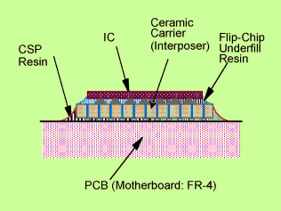
CSP was conceived from the beginning to be an underfill-free assembly. But in view of the increased stresses on the assembly expected by the move to lead-free, designers should now consider using underfills to maximize assembly reliability. Underfill acts to increase the reliability of grid array interconnects by distributing stress across the surface of the substrate instead of allowing stresses to become concentrated in the solder balls. An example of how an underfill may be used in a CSP application is shown in Figure 1. The underfill will improve compliance and reduce stress due to CTE mismatch.
 |
| FIGURE 1: Lead-free CSPs are likely to demand use of an underfill to enhance solder joint reliability. |
Lead-free CSP assemblers should now consider applying an underfill in all CSP process evaluations. Even if few applications are known where CSPs are underfilled prior to reflow soldering, certain types are known to withstand lead-free reflow up to the generally accepted maximum 260°C temperature without losing their underfill properties. These underfills appear to be applicable to lead-free CSP assembly without modification.
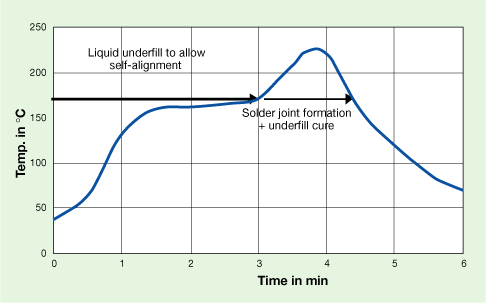
The story is slightly different for no-flow underfills, as these are applied before reflow soldering of the assembly. Their cure behavior is designed to permit the component being soldered to self-align, remaining liquid until the very peak of the reflow profile (Figure 2). If the underfill cures too early in the profile, self-alignment will be lost, and yield will fall as a result. A modified cure behavior is therefore required if no-flow underfills are to become suitable for lead-free packages. A dedicated lead-free formulation should be used if no-flow underfill is preferred.
 |
| FIGURE 2: No-flow underfill cure behavior superimposed on reflow profile; if underfill cures too early self-alignment will be lost. |
More in-depth test data are required to ascertain which CSPs are most vulnerable to poor reliability in lead-free interconnects, and to understand when a countermeasure such as applying an underfill is necessary. The non-captive packaging industry, and, to an extent, contract electronics assemblers, can expect customers to demand guarantees on lead-free CSP reliability. Whenever an assembly is switched to lead-free, therefore, it must be re-tested. This takes time, not to mention technical and human resources. The alternative is to source a complete material set for CSP assembly, including paste, as well as the most appropriate underfill. This way, end-users will not be left on their own as they seek to migrate to lead-free, a process which many are finding more complex than initially expected.
References
- Frank Ongkiehong, "CSP Underfills in Lead-Free Processes," Electronics Manufacture and Test, March 2005.
- Dr. Malcolm Warwick.
Dr. Brian Toleno is application engineering team leader, Henkel electronics group (henkel.com); brian.toleno@us.henkel.com.


