2005 Articles
Parts and Parcels
The case is growing for embedding passive devices.
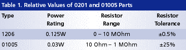
The growth in use of tiny passive components has stimulated the world’s placement machine manufacturers to develop more reliable systems capable of handling 0201 and now 01005 packages. These components are used mainly in digital, low-power circuits built in very high volumes – e.g., RF modules or mobile phones – where touchless pick-up and increased feeder index accuracy have become the norm. Such methodologies also benefit other components and tend to widen their process windows, thus making high-tech circuits in general easier to manufacture. Miniature passives carry the penalty of a reduced range of values, tolerances and dielectrics, but the most marked change is the reduced capacity to handle power and current. When comparing the 01005 with the 1206 resistor (Table 1), you can see why why the 1206 has not died out. There will always be a need for high power analog circuits and it may not always be possible to specify resistor or capacitor networks to avoid placing vast numbers of small passives. The need will remain for power and capabilities provided by larger case sizes, albeit in relatively low volume.
The passives market is evolving as follows:
0603: Standard building block.
0805: Dying out.
1206: High power, unusual tolerance, unusual dielectric but small volume.
0402: Specialized high volume with restricted range.
0201: Specialized high volume with restricted range.
01005: Specialized high volume with very restricted range networks; increasing use for reducing placement numbers and making component types easier to handle and solder; may not be suitable for RF designs.
A forecast of component use trends (Figure 1) generally bears this out, 01005s excepted. When the graph was produced it was not clear if 01005 packages would become mainstream (and it also did not include networks). However, it does include a line titled “embedded” and that is the focus of this column.
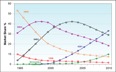 |
| FIGURE 1: One forecast predicts 0201s and EPs to supplant larger packages. (Source: Prismark) |
Embedding passive components into a PCB has been years in the making. At the start, there were no standards and materials were expensive and little understood. Most assemblers used devices no smaller than 0402 and although the process window was tighter than for larger devices, the 0402 provided a good capability for dense circuits and a reasonable range of types and power ratings. There was no strong incentive to invest in embedded technology until packages progressed to 0201 and then 01005 sizes. Networks in IC package styles also offered a means of tailoring circuit needs to reduce and simplify placement for non-RF circuits.
Embedded passives are now attractive in order to avoid placing tiny components with very narrow process windows. The technologies are better understood and CAD software is available. Standards exist for design and circuit layout and many laminate suppliers can offer suitable grades of material.
Cost and functionality. The cost of designing and manufacturing an EP board is not insignificant but the cost of 01005 components is very high. In time, economies of scale will lower the manufacturing cost of the components, yet the cost of manufacture with such narrow process windows must still be considered. Engineering cost rises when the risk of rework and failed product increases. Because the process window is so narrow, DPMO levels are higher than for larger devices and the rework skill requirements are much higher.
If the reason for specifying tiny components is to try to cram as much functionality into as small a space as possible then even though 01005s give a good area possibility, their reduced range and difficulty in processing make using the board volume a bed of R’s and C’s a very sensible way of increasing function, reducing the overall component count and increasing yield.
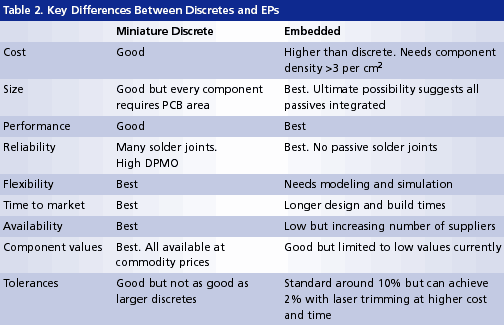
Note that EPs are only part of the equation and not a replacement for individual components. Some values, tolerances and dielectrics are not suitable for embedded technology and so there will still be a need to place large numbers of components. Also, the actives used on these circuits will probably be sophisticated and maintain the need for machines that handle and accurately place them.
Solder paste particle sizes have continually decreased in line with smaller termination sizes. Ideally, a paste deposit should be a uniform parallelepiped that does not slump and provides a stable platform for the component placed into it. In general, a high number of particles bound together in a sticky flux/solvent medium provides that base. As termination size decreases, that rule forces the particle size to shrink; today’s advanced pastes use particle sizes of around 0.015 mm diameter. Unfortunately, such tiny particles act like quicksand when printed in large volumes and the stencils necessary to print for 01005s (max 0.1 mm thick) do not suit larger components such as tantalum capacitors.
The 0201s can be soldered comfortably with component spacings of 0.2 mm and can be spaced at 0.15 mm under special circumstances. And 01005s offer the possibility of 0.1 mm spacings but, of course, the process window is narrow, leaving little margin for tolerances or errors (Table 2). Consequently, these tiny components are used mainly for high-density, low power, digital circuits such as RF transmit/receive modules in which large components are not necessary. The market for these is huge and assemblers are often niche suppliers geared for high volumes of challenging manufacturing.
Peter Grundy is director of P G Engineering (Sussex) Ltd.; peter.grundy2@btinternet.com. His column appears semimonthly.


