2005 Articles
On a Flat Note
The flat, leadless PQFN package traps flux from no-clean paste, leaving a gooey, conductive residue.
Flux volatilization is a critical factor in maintaining ionic cleanliness levels that lend to reliable performance. In a no-clean process, when the flux is activated and fully volatilized, it leaves a benign residue carrier or solvent that will not have a negative impact on field performance.
New and compact forms of IC packaging, particularly PQFN (power quad flatpack no-lead) packages, solve spacing issues for power electronics but have been shown to entrap flux residues by not permitting a volatilization path. This occurrence causes the entrapment of a high concentration of gooey flux residues that can cause product failures. Though space is saved by a smaller footprint and replacement of axial leads, potential for flux entrapment becomes a huge concern to those using this type of package.
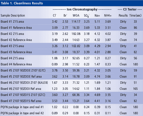
In other words, sometimes space conservation comes at a cost. A recent customer was using a PQFN package in an automotive application, and was experiencing stray voltage failures in the Z15 area where this package was located. This caused LEDs to stay on and, eventually, cause failures. Upon removing this package from the assembly, we found a visible flux residue underneath. This customer sent several assemblies for analysis to determine the source and type of ionic contamination.

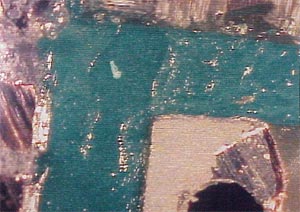
The process used was no-clean with some selective soldering sites. There were visible flux residues on the assembly, and the areas we looked at included the QFN package as well as several selective soldering sites. We also looked at the cleanliness of incoming bare boards and PQFN packages. The selective sites showed low residue levels, indicating that the no-clean flux had done its job and volatilized. The failure area around the PQFN package showed only one flux activator group, and gave readings of high weak organic acids (WOA). These residues were coming from marginal cleanliness levels of the bare board and components combined with the flux used in wave solder. These elements combined and trapped under the PQFN package create a very high risk for conductive pathways to form. To investigate this problem and process more fully, I visited the location assembling the boards with the PQFN. They used a nominal range profile for the reflow oven with the no-clean paste. We tried modifying to a higher reflow profile, but there was still gooey, non-complexed flux under the PQFN package (Figure 1).
 FIGURE 1: Area under PQFN package from a 0.006" stencil with heavy, gooey flux residue.
 |
The reason for this phenomenon is that as the weight of the PQFN package collapses over the molten solder paste during reflow, flux from the outside is sinking over and becoming trapped underneath the package where it cannot be complexed and released. The PQFN, which sits atop solder paste at a 0.006" stencil thickness, is able to drop to 0.003-0.004", thus trapping the flux and blocking the solvent path of volatilization.
To solve this, we suggested designing a 0.005" standoff to fit into the vent pipe vias that would physically hold up the part, and not permit the column of solder to collapse under the part weight. The part will hold up the solder until it cools. If this were an aluminum part, it would function as a heatsink fin.
We are now working with this customer to enact this corrective design plan, and are also working to develop a remedial cleaning protocol to remove the flux residue from underneath PQFN packages. Smaller, more compact technology is always developing at a rapid pace, and sometimes challenging cleanliness issues are being discovered. Although this part is known for its heat dissipation, great precaution is needed when incorporating PQFN packages into design to prevent flux entrapment with no path of volatilization.
Terry Munson is with Foresite Inc. (residues.com); tm_foresite@residues.com. His column appears monthly.


