Removing Markings without Stressing Components
Companies often want to have the markings on components removed to make it hard for rivals to easily find out what parts are used on the PCB.
Similarly, military and security products without product part codes make them hard to reverse engineer or hack. The problem is that this is usually done after the PCB assembly otherwise it is difficult to ensure that the board is made correctly but, the usual technique of manually grinding the markings off, is time consuming and can often damage the component and stress the solder joints. 

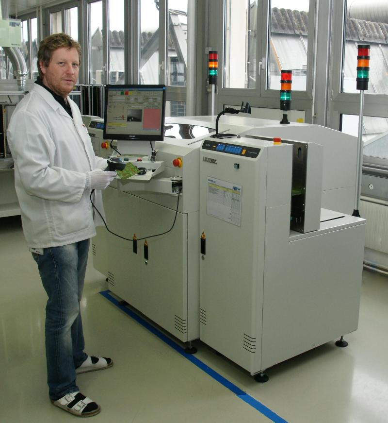
EMS firm Escatec handles this problem by using a CO2 laser marker installed to change the surface structure of the solder resist to give a clear and permanent marking on the surface of PCBs. The marking can be for machine-readable codes as well as text, graphics and logos which show up as white areas on the PCB.
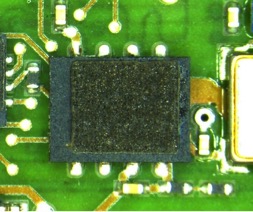
"We found that using the laser to burn on a 'sea of numbers' pattern on the tops of the components made sure that none of the markings can be read," explained Martin Muendlein, engineering manager. "There is no damage or stress and the laser is very fast and accurate to within ±0.1mm. Most important, it is fully automatic so that we cut out a huge amount of time that was previously spent grinding the markings off and therefore reduce production costs for the customer."
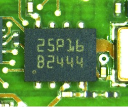
FIGURE 2, at right, shows an example of a PCB with the markings, while FIGURE 3, below, shows the same part with markings removed from the key components.


