Deeply Diagnostic Acoustic Imaging
Three less common but highly intense modes for nondestructive inspection.
Acoustic micro imaging tools look inside a sample such as an electronic component and see – nondestructively – features that can’t be imaged or analyzed by other means such as x-ray. The most common imaging modes are well known, but other, less well-known acoustic micro imaging modes are capable of more powerful diagnoses.
Most acoustic imaging systems use one of two imaging modes. In reflection mode, the tool’s ultrasonic transducer pulses ultrasound into the sample and receives return echoes of various amplitudes from material interfaces within the sample. Gap returns reflect nearly 100% of the pulse.
In transmission mode (through-scan), the transducer pulses ultrasound into the sample, but instead of reading the reflected echoes, a sensor beneath the sample receives the pulses that have traveled through the sample. Regions where no pulse arrives (because it was reflected back by a gap above) are black and identify defects.
‘Thousands of Pulses’
Several thousand times a second, the ultrasonic transducer used in acoustic micro imaging tools sends pulses of ultrasound into the component being imaged. What each pulse is “looking for” is the interface between two materials. Where there are no material interfaces (a homogeneous material with no internal defects, for example), there are no echoes.
If the two materials are solids (mold compound and silicon, for example), a portion of the pulse will be reflected as an echo. The balance of the pulse crosses the solid-to-solid material interface and travels deeper, where it may strike one or more additional interfaces.
But if one of the materials is air or another gas, virtually 100% of the pulse is reflected as an echo signal. A gap only 100Å thick between two solids is enough to cause this near-total reflection. Physically sectioning and grinding a sample and performing optical inspection may not find such a thin non-bond or delamination, but acoustically it produces the highest amplitude signal.
When more precise detail about the internal structure of an electronic component is required, other modes can do the job. Three of those modes are described here.
3V imaging mode. 3V imaging mode is used to make 3D images of interior features as they “look” to ultrasound. 3V images display the z dimension, as well as x and y dimensions. Typically 3V is used to make the overall internal structure easier to understand.
To make a 3V image, the sample is scanned by the transducer. Echoes are returned by each of the thousands or millions of x-y locations where a pulse was reflected by the interface between two solids or between a solid and air, as is found in cracks, delaminations and other gaps.
At solid-to-solid interfaces, part of the ultrasound is reflected to the transducer, while the remainder of the ultrasound crosses the interfaces and travels deeper into the sample, where it may be reflected by another material interface. But 3V is set to receive only echoes from the interface of interest selected by the user, and ignores echoes from other interfaces.
Each returning echo has amplitude and polarity, both of which give information about the materials at the interface. It also has its own time of flight, which indicates the depth of the interface from which that particular echo was reflected, and determines the height of that pixel in the 3V image.
FIGURE 1 shows a 3V image of a plastic encapsulated microcircuit (PEM). This image is shown almost entirely in monochrome to emphasize the overall structure. The square die is at the center, with the lead fingers radiating in all directions. At each corner of the component is the circular image of a mold mark in the plastic. But the most striking feature is the upward-reaching popcorn crack that begins in the mold compound region under the die and extends upward. The crack is basically circular but of uneven height; a portion at the left is marked red to indicate it has reached and broken through the top surface. Other parts of the crack do not reach so high. The portion that reaches the surface overhangs a region of the die that is black because the echoes from the crack above it reflect all the ultrasound.
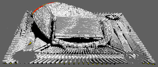
Figure 1. 3V (3-dimensional) image of a plastic-encapsulated microcircuit. Large curved structure is a “popcorn” crack.
Nondestructive cross-sectioning. PEMs and other samples are often destructively sectioned and polished to examine the cross-sectional view optically for clues to the origin of a failure. Q-BAM mode creates a parallel cross-sectional view nondestructively using ultrasound. There are two advantages to the nondestructive approach: 1) The PEM is not destroyed and is still available for electrical and other tests, including physical sectioning; and 2) the PEM can be sectioned along as many lines as desired. It can be scanned along one line, moved, and scanned along a parallel line. Or it can be rotated 45° or 90° or any other value and then scanned. Distances can be measured accurately in the Q-BAM image, a feature that can be helpful if later physical sectioning is anticipated.
To begin Q-BAM imaging, the user defines a straight line on the surface that will be the path that the transducer will follow. On the first pass, the transducer collects echoes, if any, only from the very bottom of the PEM. For the next pass, it collects echoes from a slightly higher depth. It continues this process until it reaches the surface of the PEM, at which point it will have collected all of the echoes within the vertical plane defined by the surface line. The resulting acoustic image will correspond to an optical photo of the same vertical plane if the PEM were sectioned. The vertical measurements on the acoustic image will be correct. One possible difference from sectioning: Very thin gap-type defects will be obvious (typically red) in the acoustic image, but they may be too thin to be detected in an optical image. C-SAM can image gaps as thin as 200Å, equal to 0.02µm.
FIGURE 2 is a reflection-mode acoustic image of a PEM. The echoes for assembling the image were gated on the depth from the die face down to the top of the die paddle. Red regions indicate the mold compound is disbonded from the die paddle. Yellow borders mark the very edge of disbonded regions, but larger yellow regions are caused by the scattering of ultrasound by wires extending from the die.
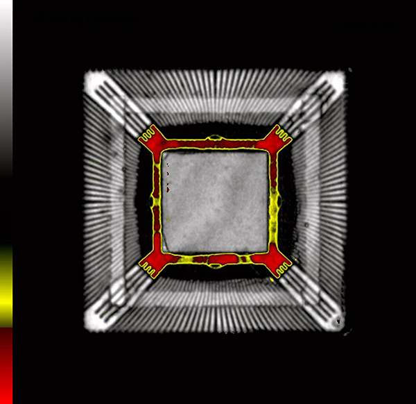
Figure 2. Reflection-mode (i.e., planar) image of a similar device. Red regions are delaminated.
The lower part of FIGURE 3 shows the top-down acoustic view of a PEM. To make the acoustic image, the transducer scanned back and forth along the scan line marked in the figure. The transducer began with the focus set near the bottom of the sample, and gradually worked its way upward to the top.
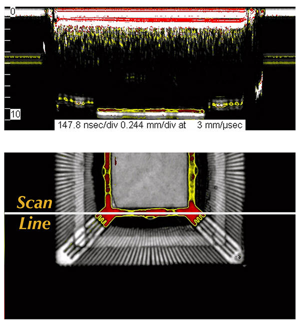
Figure 3. Bottom portion is reflection-mode image; top portion is the non-destructive cross section along the scan line.
The cross-sectional Q-BAM image occupies the top portion of the image, above the white bar that tells the 10 fine lines at the upper left each mark a division of 147.8 nanoseconds, equal to 0.244mm. The physical distance from the top of the package to the bottom of the die paddle is thus 2.22mm.
At the bottom center of the Q-BAM image is the cross-sectional view of the die paddle along the route traveled by the transducer. The mold compound just above the paddle is invisible (black). With two probable (non-red) interruptions that correspond with the planar image, this portion of the die paddle is delaminated (red) for its whole length. To the right and left of the die paddle, the Q-BAM portion shows the cross-sections of the tape and a few of the lead fingers, but no defects.
A different PEM is shown in FIGURE 4. Here, the sample has been rotated to scan corner-to-corner. What the Q-BAM image at the top shows is the die and die attach are both quite level, but small red features are at either end of the image of the die; these are die face delaminations, which are likely to expand in service and shear off wire bonds on the die.
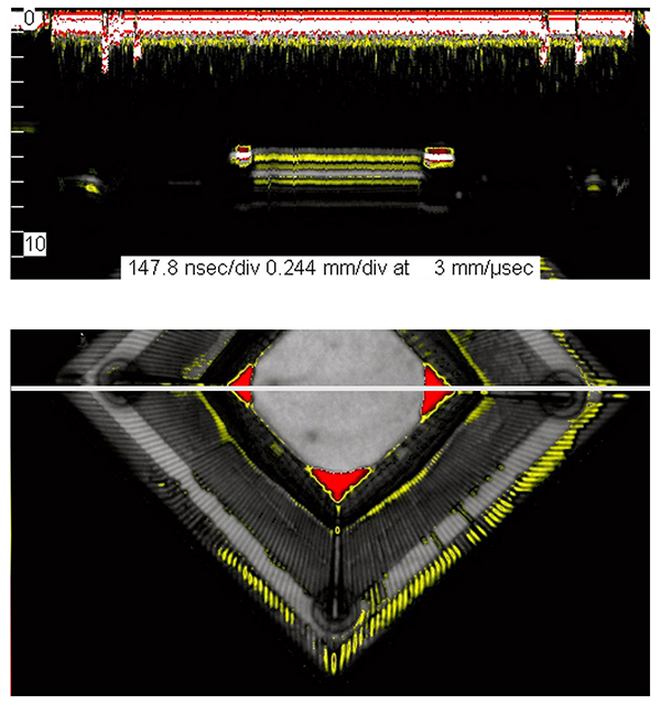
Figure 4. The same sample was rotated 45° for this non-destructive cross section.
Virtual rescanning mode. This mode diagnoses the origin of a structural failure in a component, but requires advance planning. It is used, for example, during pilot production of a new PEM, when the component as yet has no history of anomalies or failures.
Before any stress testing (thermal, shock and vibration, radiation) is performed, the plastic-packaged component is scanned by an acoustic micro imaging tool. But this is not ordinary imaging, where the goal is to find an anomaly that stands out because of its bright reflection. Instead, it is assumed there are no existing internal anomalies, and the component is scanned to collect interface echoes from all depths. A single pulse of the thousands of pulses sent per second by the transducer may send back numerous echoes at various amplitudes, arrival times and frequencies at a single x-y location – and scanning the whole volume of the component will mean millions of pulses at thousands of x-y locations. The transducer is refocused several times during scanning to avoid even slight distortions. At the end of scanning, no acoustic images are produced, but the large data file is carefully preserved. The file contains the data for every echo from every pulse that encountered a material interface within the package.
If the component suffers an electrical failure during testing or in service, the physical component will be imaged, probably by reflection mode, to get some idea of the location within the component of the structural defect that caused the electrical failure. This image made from the physical component might tell the whole story, but if it is critical to learn what caused the failure, the VRM file is retrieved. The file contains all the echoes from all the material interfaces in the physical component in its original state. Some folks call VRM the “time machine.”
A technician will use a C-SAM tool to virtually scan this file. Any depth or region in the component can be imaged. In addition to reflection-mode imaging, other modes can be used, including Q-BAM described earlier, but also several others. For example, one mode permits the user to divide the volume of the component into horizontal slices; each slice will produce a single acoustic image showing details at that depth.
Suppose the virtual file shows a small possible delamination or disbond on one edge of the die face. A mode known as frequency domain imaging (FDI) can be used to examine this small defect in its original form. FDI lets the user make an image using, for example, only echo signals whose frequency is close to 75MHz, or 80MHz, or 115MHz, or some other frequency. Images made at a variety of frequencies sometimes reveal subtle details that are not otherwise detectable. In this component, for example, FDI might reveal the delamination may already have been in contact with the wire bond when the VRM data were collected.
The PEM shown in FIGURE 5 was imaged from its VRM file, and not from the physical sample. Focusing and gating were set on the virtual file to produce an image of the depth from the die surface to the lead fingers. This PEM is notable principally for its numerous defects: a large popcorn crack surrounding the die, probable delaminations on the die, and delaminations on the distal ends of virtually all of the lead fingers. In real-world analysis of failed items, the failures are likely to be more subtle, and the need for careful and accurate analysis of the destroyed or absent component far greater.
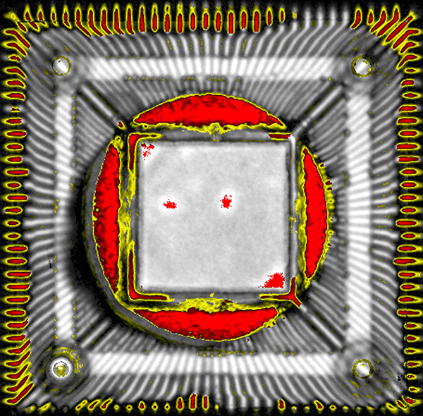
Figure 5. This image was made not from the physical sample but from its preserved data file.
is a consultant to Sonoscan (sonoscan.com); tom100adams@verizon.net.


