Improving the PCB Assembly Manufacturing Process by an Alternative Solder Paste: A Statistical Evaluation
Characterization results of several Pb-free solder pastes show one capable of low-aspect ratio printing.
Attempting to ensure sufficient paste transfer through ever-smaller apertures onto correspondingly smaller pads can result in excess paste volumes for larger apertures (0402 components and above). Excess paste volume underneath a chip component has been shown to be a significant contributor to mid-chip solder balling.1 Solder paste inspection (SPI) equipment has brought a level of control to the problem, as potential defects can be identified and the board reworked (cleaned and reprinted) prior to reflow, which minimizes cost.
Another approach for managing printing defect reduction is through adherence to IPC-7525B.2 This dictates that the area of the aperture wall be no smaller than 0.66 of the area of the pad, a measurement often referred to as area ratio or aspect ratio. The standard, however, defines only what is required for a reliable solder joint based on the ability of a typical solder paste to release from a stencil. The need to maintain the aperture aspect ratio at or above 0.66 (though some processes have been successful at slightly below this ratio) has driven use of thinner stencils and, in turn, finer powders. For example, with the standard aspect ratio, an 80µm thick stencil will require Type 5 powder simply to permit efficient filling of the aperture by the solder particles. This approach comes with a cost; Type 5 solder pastes typically require a nitrogen (N2) atmosphere for effective reflow. To accommodate both small aperture deposits alongside larger required deposits and optimize paste volume, a variety of solutions have emerged. These include step stencils, overprinting, and alterations to aperture geometry, but all have limitations. Solder paste that reliably exceeds these criteria is the first step toward the paradigm shift of board design and components driving stencil requirements, rather than the solder paste.
Despite this shift, limitations remain in the particle size of the solder paste, though this is now driven by the ability of the particles to effectively pack into the aperture. Equipment advances such as vibrating squeegees permit extensions in the use of any given particle size distribution.3 The general rule-of-thumb that the smallest aperture width used should accommodate at least five particles still informs particle size choice (TABLE 1). Once the particle size of the powder is determined, solder paste flux selection follows. This is determined by a variety of criteria, the primary factor being the substrates onto which the components will be soldered. Sometimes, however, the need for an L0 classification4 determines flux choice. This is often as far as flux consideration goes, with little thought given to flux stability and performance in the print process. To better understand flux significance, a study was performed to analyze printing performance of four different solder pastes and evaluate their printing performance as it relates to the impact on process capability.
Table 1. Minimum Aperture Size for Different Particle Size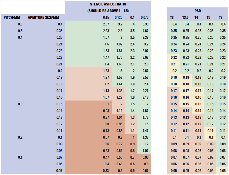
Experimental
Material selection. Four common, commercially available solder pastes were selected for this study and are summarized in TABLE 2. All the lead-free pastes are also halogen-free as defined by IPC5 and meet the IPC/J-STD 006 classification of Type 4 powder.
Table 2. Summary of Solder Pastes Evaluated
PCB design. A solder paste evaluation is only as good as the PCB, stencil and printer setup. Rather than evaluating all four pastes under the same print conditions, it was decided each paste would be processed under its optimum print conditions (as determined by each material’s TDS). With this approach, true paste performance could be evaluated, and poor performance would not be the result of printing conditions.
The test board was designed to evaluate material performance for current miniaturized components and interconnects. Intentionally, the PCB design ensured for pads that were not square or round, both parallel and perpendicular pad orientations were present for evaluation. Finally, it was necessary to consider the number of pads present on the board. A claimed 20 part per million (ppm) defect rate is not unusual in many print processes, and corresponds to one failure every 50,000 pads. To identify changes to this defect rate, a significant number of pads are required. The lack of pads on any given board can be replaced by increasing the number of boards printed. With this in mind and considering the necessary real estate required, 200 of each of the passive components were used (100 parallel and 100 perpendicular), yielding a total of 400 passive pads per board. The array components were a bit less complex to design for evaluation, as each component has several hundred I/Os, and each component is square, which means there were no parallel and perpendicular pad orientations to accommodate. Therefore, 10 of each type of array component per board were used. (See TABLE 3 for the full list of components and FIGURE 1 for the board layout.) This design yielded a total of 21,461 pads per board (excluding the ground planes for the QFN). To improve statistics and to confirm print performance consistency, 10 boards were printed for each solder paste’s optimal print condition. The array components were daisy-chained and the board designed so that each side could be probed for continuity to help locate solder defects for failure analysis.
Table 3. Test Board Pad Count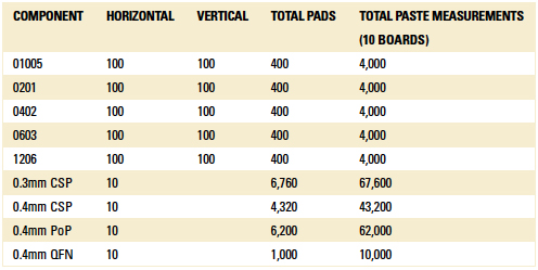
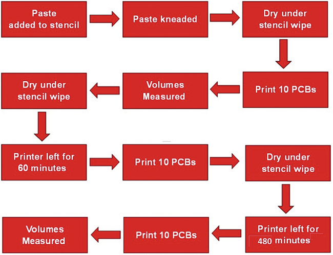
Figure 1. Test board layout.
The stencil aperture design used rectangular apertures for passive components with an area of 90% of the associated board pad, while the array components used a rectangular aperture with rounded corners. Rounding the aperture corners increases the aspect ratio over the standard rectangle (TABLE 4). Even with this adjustment, IPC-7525B has a 01005, 0.3mm CSP, 0.4mm CSP and a PoP component with aspect ratios below the recommended 0.66. To meet this criterion would require an 80µm thick stencil for the array components and a 73µm thick stencil for the 01005.
Table 4. Effect of Stencil Thickness and Shape on Aspect Ratio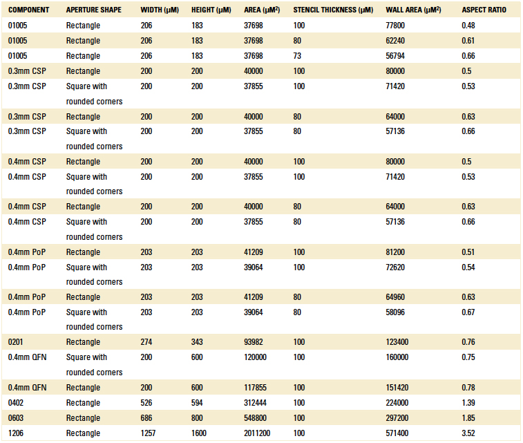
The move to thinner stencils will necessitate use of a finer powder and, with this, a likely move to nitrogen-inerted reflow, with the associated costs to the process. Therefore, it is desirable to remain with a Type 4 powder as long as possible. Consequently, this evaluation was conducted using Type 4 powder.
Equipment and Procedure
An ASM Assembly Systems’ DEK Horizon 01iX stencil printer, fitted with vacuum tooling, was used to print the selected pastes on the PCB. Boards were supported by vacuum tooling, as edge clamps were found to impact print performance up to 1.25" in from the edge of the boards. All pastes were printed under their optimum print pressure for the chosen print speed of 75mm/s-1. For each experiment, a fresh jar of solder paste was used. The paste was opened and stirred for one minute; then 250g of solder paste was weighed with a plastic weighing dish. The measured paste was then placed on the stencil in a single bead, extending approximately 25mm beyond the end of the apertures on the stencil. The paste was then subjected to a four-stroke knead cycle to fully wet out the apertures, after which a dry underside stencil wipe with vacuum was performed. Ten virgin boards were printed and the volume of the solder deposits measured. After the tenth print, the stencil was once again subjected to a dry underside stencil wipe, and the solder paste was left stationary 60 min. The second 10 virgin boards were then printed and the solder paste deposit volumes measured; again, a dry underside wipe of the stencil was performed. This time, the paste sat for 480 min. (8 hr.) before a final set of 10 virgin boards was printed and deposit volumes measured (FIGURE 2).
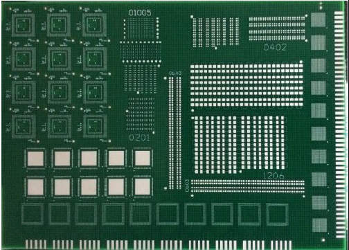
Figure 2. Experimental flow chart.
Inspection of each printed board was performed using a Koh Young 8030-2 SPI, which utilizes white light interferometry (Moiré interferometry) to measure the area and height of the solder deposit. This measurement is then used to calculate a volume for the deposit, and the measured volume is compared to the theoretical volume of the stencil aperture to yield a nominal volume in % (Eq. 1, below).
Data Analysis
Cp and Cpk values were calculated for the various materials and apertures using 100% nominal volume as the target volume and ±50% as the upper and lower specification limits. These percentages were selected based on the results of a straw poll of SPI users and reflect industry common practice rather than limits based on post-reflow defect levels. Both Cp and Cpk are process capability measures used to extrapolate collected data to determine the expected amount of data that will fall outside the desired specification limits. The higher the Cp or Cpk value, the narrower the distribution and the fewer expected defects (TABLE 5 and FIGURE 3).
Table 5. Relationship of Cpk to Defect Rates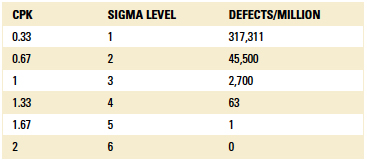
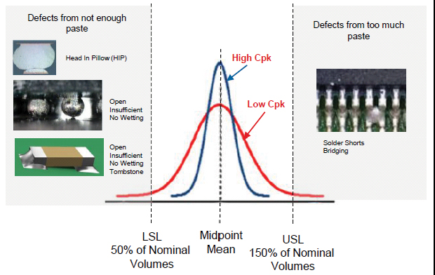
Figure 3. Graphical representation of the relationship of Cpk to defect rates.
The Cp value is a measure of the current process variation capability if the distribution is centered in the specification range. The Cpk value takes into account the actual location of the measured distribution within the specification limits. Thus, if the Cp and Cpk values are the same, then the actual distribution is perfectly centered within the specification limits. Conversely, if Cp is high and Cpk is low, this would suggest the measured distribution is shifted to one end of the specification limits and that action needs to be taken to alter the distribution. For this study’s comparisons between prints, simple box and whisker plots were used that permit a graphical comparison of the data spread from print to print.
Ed.: The results, discussion and conclusions of this study will be published in the February issue.
is associate director, Advanced Process Laboratory at Universal Instruments (uic.com); barbini@uic.com.


