Improving the PCB Assembly Manufacturing Process by an Alternative Solder Paste: A Statistical Evaluation, Part II
Characterization results of several Pb-free solder pastes show one capable of low-aspect ratio printing.
Ed.: Part 1 appeared in the January 2017 issue of PCD&F/CIRCUITS ASSEMBLY.
Results and Discussion
The fluid nature of the solder paste results in a situation where the downward force applied by the squeegee on the paste in front of it is, in part, balanced by the weight of the column of paste behind it (FIGURE 4). This will result in paste being pushed above the height of the stencil. The high viscosity of solder paste means it takes a little time to reach the equilibrium; consequently, this phenomenon is not observed for small apertures where the time the paste bead is over the aperture is short. This results in a gradual increase in the volume of paste as aperture dimensions increase (FIGURE 5A). This qualitative approach ignores the impact of release on deposit volume. Consequently, with small apertures, the volume drops below 100% for all materials, except material A, which remains around 100% of nominal volume (FIGURE 5B).

Figure 4. Effect of pressure on solder paste in large apertures.
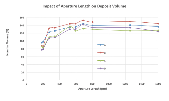
Figure 5A. Impact of aperture length on deposit volume.
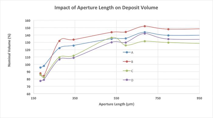
Figure 5B. Impact of aperture length on deposit volume.
Looking at the same data for deposit height (FIGURES 6A and 6B), the effect is less pronounced, except for material A. This suggests some peaking of the material, as it is pulled out of the aperture for materials B, C and D. So, for materials B, C and D, the IPC-72525B recommendation of an aspect ratio of 0.66 would be appropriate, while material A appears to be limited more by particle packing.
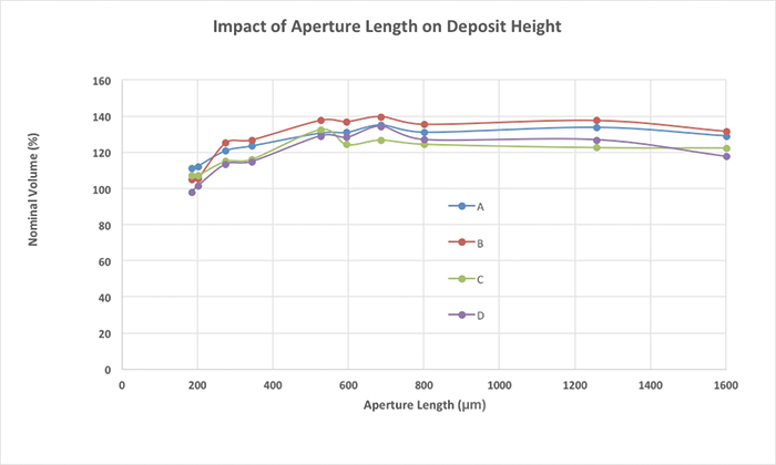
Figure 6A. Impact of aperture length on deposit height.
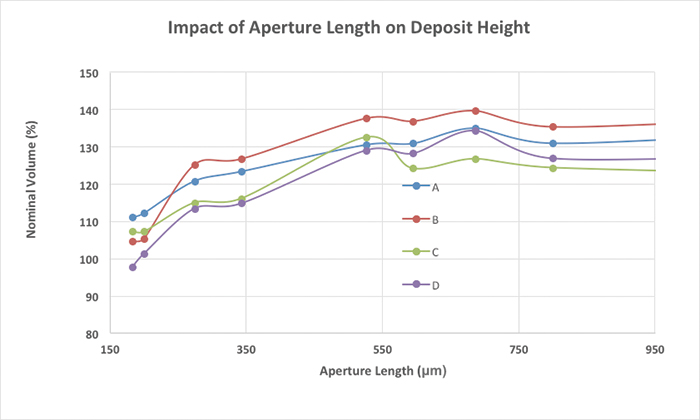
Figure 6B. Impact of aperture length on deposit height.
This phenomenon of liquid flow under pressure can also be used to explain the deposit shape for larger apertures. The exact equilibrium volume for a given paste is a combination of the aperture size, print speed, and pressure. Since the paste requires a finite time to reach equilibrium as the paste nears the end of the aperture, there is insufficient time for the paste immediately behind the squeegee to reach equilibrium. The result is a small, finite slope on the deposit in the direction of squeegee travel. For small apertures this will be across the full width of the aperture; for larger apertures, it will only be at the end of the deposit. The distance this slope extends and the print speed will determine the time required for the paste to reach equilibrium.
In addition to other contributors, this excess paste volume may lead to the generation of mid-chip solder balls. This increase in volume can be seen by looking at the shift in the volume distribution of the various component apertures. The distribution moves steadily to the right (FIGURES 7A-7D) as the component size increases. Although it is not obvious, the distribution also narrows, as can be seen by an increase in the Cp for each of the various component apertures (FIGURE 8 and TABLE 6).
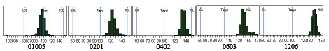
Figure 7A. Effect of component size on print volumes for Paste A. (Data are the accumulation of 10 boards printed without an underside stencil wipe, 200 components per board, 100 parallel and 100 perpendicular.)
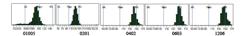
Figure 7B. Effect of component size on print volumes for Paste B.
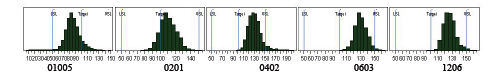
Figure 7C. Effect of component size on print volumes for Paste C.
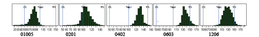
Figure 7D. Effect of component size on print volumes for Paste D.
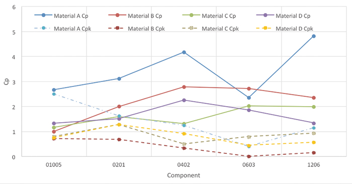
Figure 8. Effect of aperture size on Cp and Cpk.
Table 6. Effect of Aperture Size on Cp and Cpk for Different Solder Pastes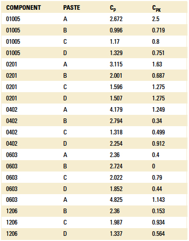
Unfortunately, gains in Cp are more than offset by the movement of the distribution away from the center of the specification range, as shown by the drop in Cpk. In most cases, the practical impact of this additional volume can be seen by the presence of mid-chip solder balls, which have been shown to be related to the volume of paste deposited. It is the excess paste in large apertures that results in the defects and the drop in Cpk. For small apertures (0201 and below), it is the poor release that yields insufficient solder paste and lowers Cpk values for pastes B, C, and D; thus 0201 and 0402 components are optimum for most pastes.
The insufficient solder paste resulting from poor release of small apertures with low aspect ratios has received more attention because the solution is more complex (reducing the stencil thickness and using a finer solder powder). However, the data for paste A clearly show an increase in Cpk, even though there is a widening of the volume distribution. This is achieved by centering the distribution at 96.8%, close to the target volume of 100%, while the other materials are centered at lower volumes (Paste B 86%, Paste C 84.2%, Paste D 78.3%). This, combined with wide distributions, translates to Cpk of below 1.0 for the latter materials, while paste A has a much narrower distribution and achieves a Cpk of over 2.0 (less than one ppm defect rate). An aspect ratio of 0.53 would be expected to yield improved consistency. However, the change in aperture shape from a rectangle to a square with rounded corners appears to counter the expected advantages of the new aspect ratio. This suggests that not all apertures perform equally with respect to release and that the aperture aspect ratio may be an over-simplification when values are below 0.66. Particle packing may be more of an influence.
The test board has two sets of 200 by 200µm apertures in two different locations. One is for the 0.3mm CSP, and one is for the 0.4mm CSP. Comparison of the average deposit volumes for the different locations shows a significant difference in volume and consistency, which isn’t easily understood. The most likely explanation of this effect is the pin tooling used. The 0.3mm CSP was at one end of the board, while the 0.4mm CSP was along the side close to the transfer rails, which provided additional support and improved gasketing. This difference requires further study. However, the performance of the 0.4mm CSP pads rather than that of the 0.3mm CSPs should be considered to be the optimum performance of each paste.
Pastes A and B are the only pastes with Cpk greater than 1.00, or 3 sigma level (2,700 defects per million). Paste B has an average volume close to the nominal value of 100%. However, it has a long tail of low-volume deposits that brings down the Cpk to 1.12, below most manufacturing specifications of the four-sigma level of 1.33 (63 defects per million). Again, paste A yielded higher average paste volumes and higher Cpk values than those of the other three materials (FIGURES 9A-9D and TABLE 7). Pastes C and D had Cpk values of less than 1.00, indicating defect levels greater than 2,700 per million. Since pastes C and D had average volumes significantly below the target values and Cpk values of less than 1.00, it suggests that neither of these pastes is able to produce a capable or viable process (a Cpk of greater than 1.33, or four sigma). These apertures on a 100µm stencil would require the user to source a thinner stencil and a finer powder to achieve the desired result. Even paste A was below 1.33 Cpk for the 0.3mm CSP component apertures, although it achieved better than 5σ for the same apertures elsewhere on the board. This result only serves to reinforce the importance of correct tooling support for boards.
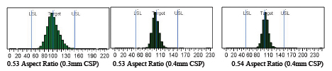
Figure 9A. Print volume distributions for low aspect ratio square apertures with rounded corners (Paste A).
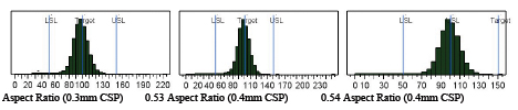
Figure 9B. Print volume distributions for low aspect ratio square apertures with rounded corners (Paste B).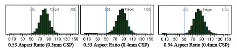
Figure 9C. Print volume distributions for low aspect ratio square apertures with rounded corners (Paste C).
Figure 9D. Print volume distributions for low aspect ratio square apertures with rounded corners (Paste D).
Table 7. Effect of Aperture Aspect Ratio on Average Deposit Volumes and Cpk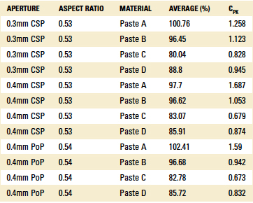
Finally, the ability of the paste to remain on the stencil and still be capable of printing must be considered. Since neither pastes B, C, or D yielded a capable process, only the data for paste A will be considered in depth. After 1 hr. without printing, the initial print for all pastes produced unacceptable levels of deposits with insufficent solder paste (FIGURE 10). The second print yielded paste volumes equivalent to those observed for the initial prints. This situation was exacerbated by leaving the paste on the stencil for an additional 8 hr. Pastes A, B and C required four prints to return to initial volumes, while paste D required 5 (FIGURE 11).
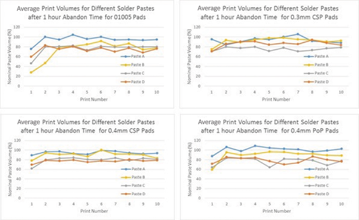
Figure 10. Effect of one hour abandon time on deposit volumes.
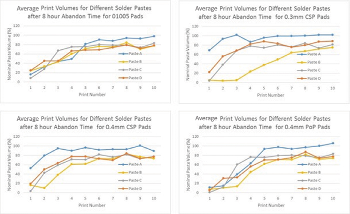
Figure 11. Effect of eight hours abandon time on deposit volumes.
However, as discussed previously, the average volume is not necessarily a good indication of a process being in control. Rather, the Cpk value, which includes both the average and the distribution of deposit volumes, is a much better indication of a material’s process capability. The Cpk values for paste A were calculated using the last nine prints after 1 hr. of abandon time and the last six prints after 8 hr. of abandon time. The data show paste A’s performance remains consistent (TABLE 8 and FIGURES 12 and 13), which suggests any residual material in the apertures does not exhibit excessive drying, which can inhibit release. The paste is capable of achieving a four sigma process and, in a number of cases, five and six sigma processes were achieved. It is likely five sigma is possible with optimized tooling.
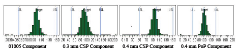
Figure 12. Effect of one hour abandon time on deposit distributions for apertures with aspect ratios below 0.66.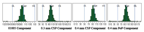
Figure 13. Effect of eight hour abandon time on deposit distributions for apertures with aspect ratios below 0.66.
Conclusion
Although significant differences in performance were observed across the different pastes, a number of common trends were documented. As aperture size increases, the deposit volume distributions typically narrow (Cp increases), eventually stabilizing for component apertures of 0402 and above. All pastes exhibited a reduction in process capability (Cpk decreases) with increasing aperture size due to a shift in the center of the deposit volume distribution to above the 100% target. This is a result of the hydrostatic characteristics of solder pastes and yields deposits that are higher than the thickness of the stencil. The extra paste may also contribute to mid-chip solder balling. Paste A consistently yields the greatest Cp and Cpk values compared to the other pastes.
For apertures with aspect ratios less than 0.66, only paste A was able to yield sufficient deposit volumes to produce a viable process, even down to 01005 apertures with aspect ratios of 0.46. Aperture shape was found to be significant, as square apertures with rounded corners and higher aspect ratios performed more poorly than the 01005 rectangular apertures.
All pastes required an initial print after 1 hr. of inactivity, and multiple prints after 8 hr., to return the average print volumes experienced on the initial prints. Cp and Cpk values for paste A also returned to similar levels as those achieved for the initial prints.
References
1. M. Currie, N. Poole and W. O’Hara, “An Investigation into the Factors Influencing Mid-Chip Solder Balling and Techniques for Their Elimination,” IPC Assembly and Reliability Conference Thailand, April 2016.
2. IPC-7525B, Stencil Design Guidelines, October 2011.
3. C. Ashmore, M. Whitmore and J. Schake, “Big Ideas on Miniaturization,” IPC Apex Expo, February 2013.
4. IPC/J-STD-004B, Requirements for Soldering Fluxes, December 2008.
5. IPC/J-STD-006, Requirements for Electronic Grade Solder Alloys and Fluxed and Non-Fluxed Solid Solders for Electronic Soldering Applications, January 2006.
Ed.: This article was originally published at SMTA International and is published here with the author’s permission.
is associate director, AREA Consortium at Universal Instruments (uic.com); barbini@uic.com.


