Imaging and Analysis Using Matched Acoustic Tools
For more complex parts such as stacked die, ultrasound can boost yield and cut costs.
When it comes to internal inspection of products ranging from simple plastic packages to stacked die wafers, it is the business of acoustic micro imaging (AMI) tools to inspect these samples without causing damage or affecting the results. The inspection technique works by the tool’s transducer pulsing ultrasound into thousands or millions of x-y locations making up the sample area. Some of the ultrasound will reflect at the sample’s surface, and some will transmit into the sample. The reflections and corresponding intensity are put in an oscilloscope display. Each echo corresponds to a depth within the sample. The transducer collects these reflections and generates a 2D or 3D image based on the signal intensity at each x-y location.
Samples compatible with AMI can vary in structure and size but are generally nonporous solid materials that conduct sound well, a description that encompasses many electronic devices and modules. The purpose of acoustic imaging is typically to locate, image and analyze internal defects. These can include cracks, voids, delaminations or non-bonds that contain air, another gas or a vacuum. The interface between a solid and air is an efficient reflector of ultrasound. An air-filled gap will reflect nearly 100% of the ultrasound and create a very large return echo. The amplitude of this echo is measured and given a pixel value in the image. Typically, images are generated such that an air cavity (defect) will appear as bright white in a reflection mode image.
The same air cavity could be imaged using the transmission imaging mode, where ultrasound pulsed by the transducer is received by a sensor beneath the sample. The internal air cavity would block transmission, and none of the ultrasound would arrive at the receiver transducer positioned under the air cavity. The phenomenon is known as shadowing. The non-arrival of transmitted ultrasound makes the air gap black in the transmission image.
The above describes the two chief imaging modes, reflection and transmission, in confocal scanning acoustic microscopy tools. Since the invention of the basic C-SAM microscope, about 15 additional imaging modes have been developed for these tools. Some of these imaging modes can be specialized to a particular product or sample. Together these imaging modes permit nondestructive imaging of a range of production items. Unlike x-ray technology, ultrasound is sensitive to an air gap and can give depth information. Its greatest appeal is to quality control, reliability and failure analysis departments.
Early work tended to involve imaging small quantities of components. But the first experiment in mass acoustic imaging of electronic devices had been conducted even before these tools were produced. Within a few years, systems were available that handled and imaged the larger number of samples transported in JEDEC-style trays with growing degrees of automation. High throughput was a necessity due to the volume of devices in demand for AMI.
Eventually the need arose for calibration and standardization among companies that were expanding or improving their quality control and automated inspection techniques across multiple plants. Soon technicians in plant A were discussing acoustic images of a device with technicians in Plant B, who were imaging the same device. It was noted between the plants that the images were not an exact copy in terms of both the features displayed and the signal intensity of the pixel levels in the image. This made discussions about the interpretation of the images difficult because the tools in use were not producing the same data. What was needed was a way for multiple tools across multiple locations to image the same sample with the same output in terms of image and data interpretation.
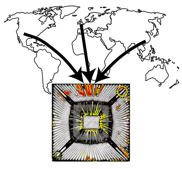
A multi-year effort led to the creation of the technology that would reliably produce identical images of the same part when imaged by multiple AMI tools at multiple locations. FIGURE 1 demonstrates the concept on a global scale, although the technology is essentially the same when multiple tools are in a single location. Development was helped by prior experience with the requirements for imaging diverse sample types and with specialized applications that would not be well served by a standard model. Also helpful was expertise in designing and manufacturing all of its high-frequency electronics and ultrasonic transducers of 50MHz and above (i.e., all the midrange and high-resolution transducers). High-throughput AMI tools may range in frequency from 15MHz to 230MHz, with 230MHz being the highest resolution production-floor friendly frequency, although laboratory tools may reach up to 400Hz.

Figure 1. Given the same component, any number of C-SAM matched tools will produce exactly the same image.
Today, matched tool systems are at work around the world. The scanning of a given lot of parts uses a recipe containing the scanning and analysis parameters chosen for this particular family of parts. Prior to scanning, the calibration software checks and verifies the performance of the transducers and analyzes signals collected using a calibration sample. If the software finds anomalies, it will disqualify the tool and notify the user via onscreen alarms and SECS-GEM communication to a host.
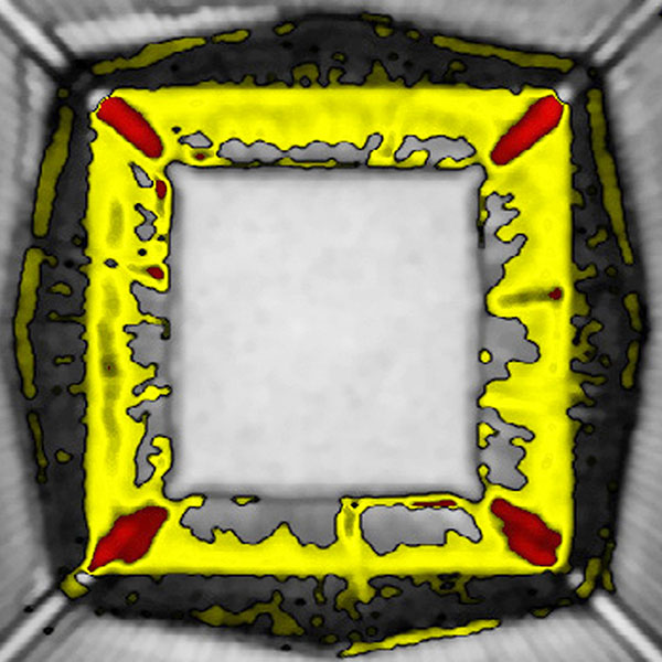
In practice, matched tool systems are able to generate matched data so that defects in a particular sample type on one tool look the same as defects in that same sample type on another tool, and can be interpreted using the same guidelines. FIGURE 2 is the C-SAM reflection-mode image of a component that has possible anomalies. Yellow regions surrounding the die are likely simply diffraction of ultrasound by the bond wires, but the red regions along the lead fingers are defects. This is a good example of a component where matched tools would make the accept/reject decisions more clear-cut because the part’s image would be the same, down to the finest details, at whatever location it was imaged.

Figure 2. Image fidelity results in more successful accept/reject analyses.
Matched tool technology is typically incorporated into high-throughput automated systems, which can image any JEDEC tray-friendly part. SECS-GEM may be used to communicate with a central database or with a server.
With the increasing demand for smaller electronics, many manufacturers have started stacking die vertically to conserve space. Stacked die are typically imaged in transmission mode due to their complexity; however, the matched tools are able to scan a particular layer if there has been a history of defects involving a particular die level. Typically a die stackup consists of eight or fewer die, but a more complex die stackup can consist of up to 64 die.
For some parts, it makes sense to use reflection mode imaging and transmission mode simultaneously. This technique uses two transducers for each inspection channel. The pulsing transducer sends and receives reflections from the topside of the sample, while the receiving transducer is positioned underneath the sample and collects signals that have transmitted through the entire sample. If the transmitted signal shows a shadow, then the reflection mode image may be able to give a depth location to that defect. However, due to the complexity of samples, typically in reflection mode a considerable number of depth-specific images may be generated to focus through the entire thickness of the part. That is why the transmission signal is also imaged at the same time – to expedite the screening process as a simple pass/fail, and then permit a more in-depth layer-by-layer analysis in reflection mode that will not slow down the production line.
Depending on the user, some parts are scanned more than once as they are built. A processor, for example, may first be imaged when it consists of a bare die bonded to its substrate. At this stage of the process there is nothing blocking the bare silicon die, and there is accordingly little attenuation when imaging the bond at 230MHz. The reason for an acoustic image at this stage is a very attenuating epoxy encapsulant and thermal interface material (TIM) are placed on top of the die, and a tin lid is later attached to the part. It is imaged again, but this time (due to the attenuation of the TIM) the frequency is dropped to about 15MHz.
The resolution and detail are both much lower than at imaging the bare die. However, 15MHz is still able to determine if any defects exist between layers at the final stage of the process.
The overall impact of matched tools is to remove ambiguity from imaging and analysis steps in inspection. Without ambiguity, truly defective devices can be clearly identified and removed as soon as possible. Earlier identification and removal translates directly into higher yield at lower cost.
is a consultant at Sonoscan (sonoscan.com); info@sonoscan.com.


