The Importance of Stencil Tension for High-Yield SMT Printing
Would higher stencil tension improve paste volumes on nickel and stainless steel foils?
The printing process is well-known to assemblers and incorporates a wide variety of inputs (stencil, solder paste, squeegee pressure, alignment accuracy, etc.) to deliver a good result. Using a squeegee and metal stencil, which is designed with aperture openings that correspond to the size of the pads on the printed circuit board (PCB), the printer facilitates the accurate deposition of solder paste onto the PCB in tightly controlled volumes. The goal is to print a calculated volume of paste in a preferred shape onto a precise point of the PCB, continuously and repeatedly.
The actual material transfer is broken down into two parts: the aperture filling phase and the material release phase. The hydrodynamic pressure (filling pressure) created by the squeegee system is crucial to successfully filling an aperture. To ensure the aperture is correctly filled, there are several factors to consider and tradeoffs to be weighed. The simplest approach, yet perhaps not most effective, is to increase all parameters that produce the highest filling pressure. Such a process might set the squeegee angles at 45° or less, establish a high print pressure and traverse at low print speeds. This would yield a high filling pressure, but would result in some adverse effects:
- The high squeegee pressure combined with a low angle leads to abrasion, which may cause damage to the stencil foil, such as deformation or coining.
- High squeegee pressure may also reduce the tension of the stencil foil, which could result in poor gasketing, misregistration and/or poor print definition.
- The high filling pressure, combined with the compromised foil integrity, may cause the solder paste to breach the gasket between the stencil and PCB, creating a “wet bridge” between neighboring apertures. This deformation of the foil could lead to insufficient material volume for ultra-fine-pitch devices too.
In addition to the damage that can be caused by higher pressures and slower speeds, continuous use under these conditions tends to degrade stencil quality more quickly and reduce foil tension. This, in turn, results in unreliable and uncontrolled material release. This article investigates how stencil tension and condition of the foil influence the overall printing process.
Design of Experiment
The test board represents a current mobile phone product and contains several component pads of different sizes, including fine-pitch devices such as 0.4mm and 0.5mm CSPs. TABLE 1 lists the equipment specifications and test parameters used in the experiments.
Table 1. Print Parameter Summary
Two stencil mounting systems were used: a 23" x 23" DEK VectorGuard Standard Tension frame (ST for future reference), and a 23" x 23" DEK VectorGuard High Tension frame (HT for future reference).
Also, two stencil foils were used: 23" x 23" 100µm thick Nickel VectorGuard foil (Ni for future reference), and 23" x 23" 100µm thick Stainless Steel VectorGuard foil (SS for future reference).
Mesh-mounted stencils remain the most commonly used stencils on the market today. However, when evaluated as part of the study, some distinct disadvantages of mesh-mounted stencils were highlighted. Densely populated PCBs and fine printing features make planarity and consistency from frame-to-frame important. Variation in foil planarity or frame integrity negates any established stencil printer equipment precision.
Indeed, there are well-known variations in the quality of tubular stencil frames, depending on the manufacturing protocols. Many frame manufacturers use extruded aluminum frames with a very thin wall thickness to minimize cost. These frames can’t be stretched to high mesh tensions because the sides of the frames will bow inward, thus reducing the mesh tension. FIGURE 1 shows some parameters to be considered for mesh-mounted frames.

Figure 1. Typical characteristics of a mesh-mount frame.
Other concerns include the foil flatness, gluing variability in height on the mesh to frame, or gluing variability on the foil to mesh.
Consistency in tension can be addressed by moving away from conventional mesh-mounted systems and evaluating interchangeable foil-mounted solutions (separate foils used with a single, tensioning frame). These stencils have no mesh, with the foil tensioned mechanically. Air bladder systems are also used for tensioning. This approach, however, can lead to inconsistent tensioning during print cycles, as initial inflating of the system is operator-dependent, and the bladders can lose pressure over time. Mechanical tension delivers extreme consistency and aperture registration accuracy that is often superior to traditional framed stencils.
To analyze the effectiveness of frame-mounted foil systems, an evaluation was conducted using two such technologies: one in standard tension similar to that of
mesh-mounted stencils (FIGURE 2) and one in high tension to deliver greater tensioning force (FIGURE 3).

Figure 2. Characteristics of standard foil-mounting tensioning system (ST used in the experiment).

Figure 3. Characteristics of a high-tension foil-mounting tensioning system (HT used in the experiment).
Ten different experiments were undertaken, as highlighted below (HT = high tension, ST= standard tension, SS = stainless steel):
- Print new Ni foil with HT
- Print new Ni foil with ST
- Print new Ni foil, tension dropped close to the ST tension
- Print worn Ni foil with HT
- Print worn Ni foil with ST
- Print new SS foil with HT
- Print new SS foil with ST
- Print new SS foil with tension dropped by the same amount as on Ni, but in this case on ST
- Print worn SS foil with HT
- Print worn SS foil with ST
Testing was conducted with a new stencil and again after 10,000 dry cycles to understand the effect that process usage has on the volumetric output.
The same 20 PCBs were printed and inspected on a Koh Young solder paste inspection (SPI) machine. Between each print, a dry clean sequence was carried out.
Results
The data were collected and grouped into two categories: nickel stencils in group 1 and stainless steel stencils in group 2. (Note: Due to the challenging area ratio and overall significance of the 0.4mm CSP, this device was investigated independently.)
The area ratio of the 0.4mm CSP was 0.6 for the Ni stencil, whereas on the SS foil the area ratio was 0.55.
Volume transfer efficiency (VTE%) was used to measure process output.
The 0.4mm CSP results with the nickel stencil are illustrated in FIGURE 4. This CSP contains 560 single data points per board, which provides 11,200 data points for analysis.
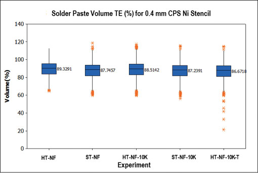
Figure 4. Different stencil experiments; solder paste volume transfer efficiencies on 0.4mm CSPs using a nickel stencil.
Figure 4 shows no significant average VTE difference among the five stencil experiments. The HT-NF-T experiment does show a number of deposits which clearly fall
below 60% VTE. These are the deposits the SPI would identify as insufficient volume.
As a general observation, the HT-NF gives the highest VTE% with the lowest spread.
The same trend can be observed with the SS stencil (FIGURE 5), but due to the lower area ratio, there are more deposits under the 60 to 70% limit. As before, the HT-NF paste VTE is the highest; however, the deviation in this test is significantly larger. The standard tension stencil produced the worst results.
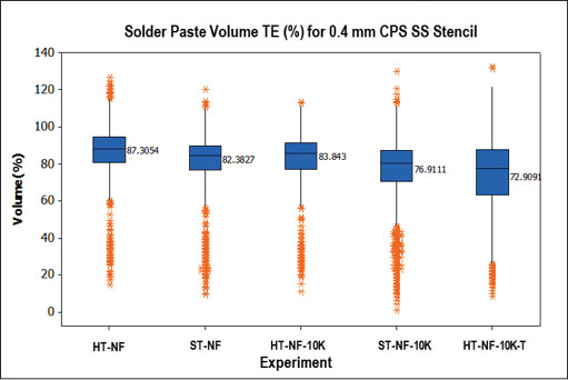
Figure 5. Different stencil experiments; solder paste volume transfer efficiencies on 0.4mm CSP using a stainless steel stencil.
Analyzing the other components, a significant difference cannot be observed (FIGURES 6 and 7).
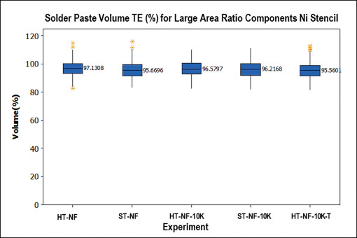
Figure 6. Different stencil experiments; solder paste volume transfer efficiencies on larger components using a nickel stencil.
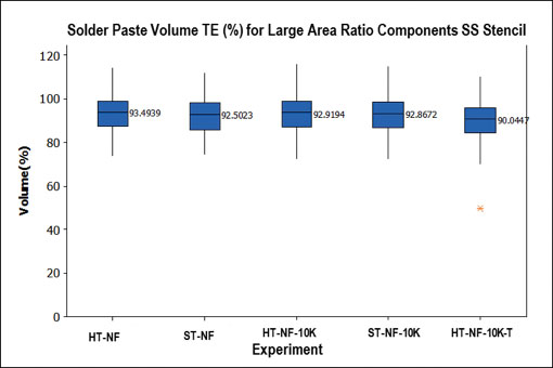
Figure 7. Different stencil experiments; solder paste volume transfer efficiencies on larger components using stainless steel stencil.
When analyzing the larger apertures, there was no apparent difference in results between the SS and standard Ni on either the standard or high-tension stencils.
However, when analyzing the stencils from a different perspective, and filtering the deposits where the VTE% does not reach a 70% limit, there are significant findings. The 70% VTE was chosen during this analysis, as it is the threshold that generates acceptable interconnects. Examining the data for those deposits below 70%, the results in FIGURE 8 were observed.
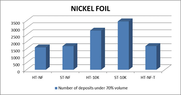
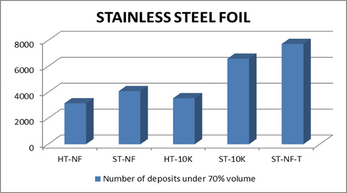
Figure 8. Number of all deposits in the population having less than 70% solder paste volume transfer efficiency on the nickel and stainless steel stencil.
TABLE 2 highlights the specific results for all components for both the nickel and stainless steel stencil. Analysis of the data yielded the following observations:
- In each case, compared to the standard-tension frame, the high-tension frame with new foil resulted in fewer deposits below the range of 70% (or less) volume.
- In each case, the worn foil (cycled 10,000 times) performed better in the high-tension frame than in the standard frame. Transfer efficiency results deteriorated when frame tension was reduced.
- In many cases, the high-tension frame with a worn foil achieved better results than the standard frame with a new foil.
Table 2. The Number of Deposits in the Population Below the Solder Paste Volume Transfer Efficiency Limit for Each Experiment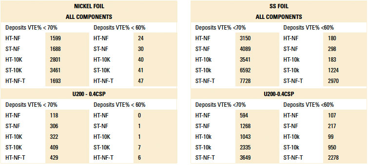
The data suggest stencil tension plays a critical role in enabling a robust and repeatable printing process. In addition, it was observed that solder paste volumes printed with a worn Ni foil were significantly different from those printed with a stainless steel foil. Whereas the harder Ni stencil does not coin, coining and deformation appeared on the stainless steel foil parallel to the printing direction. Coined stencils can result in harmful effects such as poor stencil gasketing or possible generation of lint during the under-stencil cleaning process.
Summary
This analysis illustrates that stencil tension – particularly with more miniaturized devices – is an important component in a reliable printing process. Foil wear was also determined to be a contributing factor to print integrity.
TABLE 3 illustrates the percentage difference within the inspected range of solder paste volume transfer efficiency for all components, comparing the high tension frame against the standard tension frame on new foils and worn foils of both stainless steel and nickel construction.
Table 3. Percentage Difference Between Experiments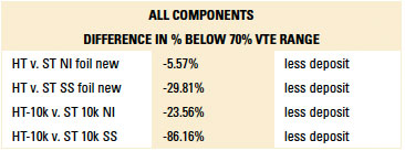
- Based on the experiments, the results indicate that higher stencil tension generates fewer occurrences of less than 70% volume range both on the nickel and stainless steel foils.
- As the aperture size decreased, the benefit of a high tension foil can generate VTE% advantages in ultra-fine-pitch component printing.
- In the case of worn foils, the difference is significantly higher with the HT and ST frames than with the new foils. CA
Bibliography
1. IPC-7525, Stencil Design Guidelines, May 2000.
2. C. Ashmore, M. Whitmore and S. Clasper, “Optimizing the Print Process for Mixed Technology,” Surface Mount Technology International, October 2009.
3. R. Mohanty, “What’s in a Squeegee Blade?” Circuits Assembly, May 2009.
4. G. Babka, S. Zerkle, F. Andres, R Raut, W. Bent and D. Connell, “A New Angle on Printing,” Global SMT & Packaging, February 2009.
5. G Burkhalter, E. Leak, C. Shea, R. Tripp and G. Wade, “Transfer Efficiencies in Stencil Printing,” SMT, May 2007.
6. I. Fleck and P. Chouta, “A New Dimension in Stencil Print Optimization,” Surface Mount Technology International, September 2002.
7. W. Coleman, “Stencil Technology and Design Guidelines for Print Performance,” CIRCUITS ASSEMBLY, March, 2001.
8. W. Coleman, “Paste Release vs Print Area Ratio,” IPC Apex, February 2001.
9. W. Coleman and M. Burgess, “Stencil Performance Comparison / AMTX Electroform vs Laser-Cut Electroform Nickel Foil,” Surface Mount Technology International, October 2006.
10. C. Läntzsch, “Nano Coated SMT Stencil with Anti-adhesion Effect,” EPP, September 2008.
11. D. Manessis, R. Patzelt, A. Ostmann, R. Aschenbrenner, H. Reichl, A. Axmann and G. Kleemann, “Evaluation of Innovative Nano-Coated Stencils in Ultra-Fine Pitch Flip Chip Bumping Processes,” IMAPS 41st International Symposium on Microelectronics, November 2008.
12. M. Whitmore and C. Ashmore, “New Developments in Broadband Printing Techniques,” SMTA International, October 2010.
13. M. Whitmore and C. Ashmore, “The Development of New SMT Printing Techniques for Mixed Technology (Heterogeneous) Assembly,” 34th International Electronic Manufacturing Conference, November 2010.
14. M. Whitmore and C. Ashmore, “Developments in Stencil Printing Technology for 0.3mm Pitch CSP Assembly,” IMAPS 44th International Symposium on Microelectronics, October 2011.
15. IPC-7525B, Stencil Design Guidelines, October 2011.
Ed.: This article was first presented at SMTA International in October 2017 and is reprinted here with permission of the authors.
is manager, process support product sales Americas and is process support product sales support engineer , CEE and EMEA at ASM Assembly Systems (asmpt.com); mike.burgess@asmpt.com.


