Fill the Void III
While voiding for QFNs tends to decrease with smaller powder sizes, stencil design plays a role.
Ed.: This study is part three in a series of papers on voiding in solder joints and methods for mitigation of voids. The first was published at SMTAI in 2016, the second at IPC Apex Expo in 2017.
Voids are gaps in a solder joint where solder does not completely fill the space between the component and circuit board (FIGURE 1). Voids have a variety of causes. Often voids are created by the interaction between multiple factors (FIGURE 2). Many of these factors were tested in previous work2,3:
- A variety of solder pastes were evaluated for voiding potential.
- Solder powder size and manufacturer were varied.
- Stencil design on QFN thermal pads was modified.
- The surface finish on the circuit boards (ENIG and OSP) was varied.
- Multiple reflow profiles in the convection oven were used.
- Nitrogen was evaluated in convection reflow.
- Vapor phase reflow was used, with and without vacuum.
All these factors were compared and contrasted with respect to voiding.
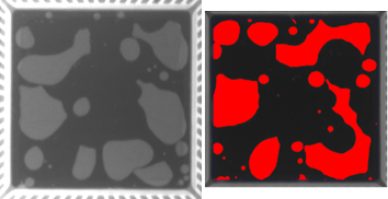
Figure 1. Voiding in QFN thermal pad solder joints.
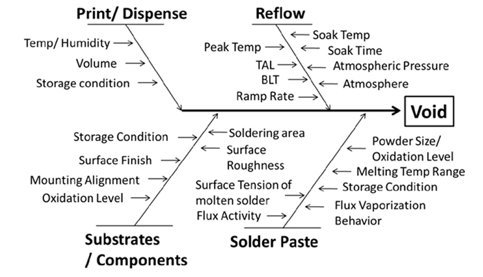
Figure 2. Factors that influence voiding.1
This investigation continues previous work and expands on the factors that were tested. Solder powder size was originally tested with one solder paste flux, and voiding levels were shown to decrease with decreasing particle size. This work was repeated with a different solder paste to determine if the voiding reduction applies to multiple solder pastes. In previous work, SAC 305 was the only solder alloy tested. In this work, SN100C alloy, SN100CV alloy, and a mixture of SAC 305 and SN100C (AT mixture) were evaluated for voiding performance. The voiding impact of electroless nickel immersion gold (ENIG) versus organic solderability preservative (OSP) surface finish was expanded to include additional solder pastes. A new “low-voiding” no-clean solder paste was evaluated for voiding performance and compared to industry standard solder pastes. Finally, stencil design was further investigated with respect to voiding on QFN thermal pads. Voiding over an eight-hour stencil life was not included in this work, but is planned for future studies.
Experimental
This experiment uses a test circuit board called Print and Reflow Test Board (PR Test Board) (FIGURE 3). This board is made of FR-4 with etched copper pads with an ENIG surface finish. OSP surface finish was also used in some tests for comparison to ENIG.
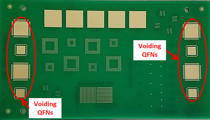
Figure 3. PR test board voiding areas.
The PR test board has four 10mm QFN-68 and four 7mm QFN-48 components. The components used were “dummy” components with a matte tin finish. Voiding was measured on the QFN thermal pads.
The solder pastes used in this study were chosen for their voiding potential. Water-soluble lead-free solder paste B has relatively high voiding potential and was used for most of the experiments. Solder paste B was used to increase the scale of measurement in order to compare and contrast factors that contribute to voiding. No-clean lead-free solder paste C was chosen because it has low-voiding potential. Solder paste C was used as a low-voiding comparison to solder paste B in some experiments. No-clean lead-free solder paste F is a new product formulated with “ultra-low” voiding potential. Solder paste F was compared to solder paste C in some experiments in order to demonstrate the lowest possible voiding.
Solder alloy was varied in this study to determine the effects of alloy on voiding. The alloys used are listed in TABLE 1.
Table 1. Solder Alloys Studied for Voiding Potential
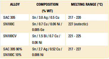
These solder alloys were chosen due to the differences in their melting ranges. In theory, wider melting ranges permit slower freezing behavior, which gives more time for gas bubbles to escape the solder joints. This theory was evaluated through voiding measurements.
Two different stencil designs were used for the QFN thermal pads. The stencils were made of 127 micron (5 mils) thick fine grain stainless steel. No nanocoatings were used. The first stencil design used a standard nine-window pane cross-hatch on each QFN location (FIGURE 4).
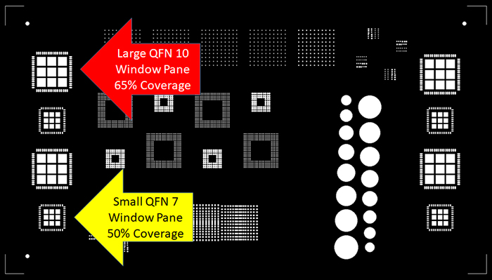
Figure 4. First stencil design with standard cross hatch on QFN thermal pads.
The board design for the QFN thermal pads was as follows: The large QFN thermal pad was 8.30mm (327 mils) square. The small QFN thermal pad was 4.90mm (193 mils) square. The stencil design for the QFN thermal pads was as follows: The large QFN cross-hatch pattern had nine 2.24mm (88 mil) square windows and a 0.51mm (20 mil) wide web for a net of 65% area coverage. The small QFN cross-hatch pattern had nine 1.15mm (45 mil) square windows and a 0.38mm (15 mil) wide web for a net of 50% area coverage.
The second stencil had different cross-hatch designs at each QFN location (FIGURE 5). The second stencil design details for each QFN location are shown in TABLE 2. The number of windows and size of windows was varied at each location to generate a certain area of solder paste coverage. The solder paste coverage area was varied at 80%, 70%, 60% and 50% for both the large (10mm) and small (7mm) QFNs.
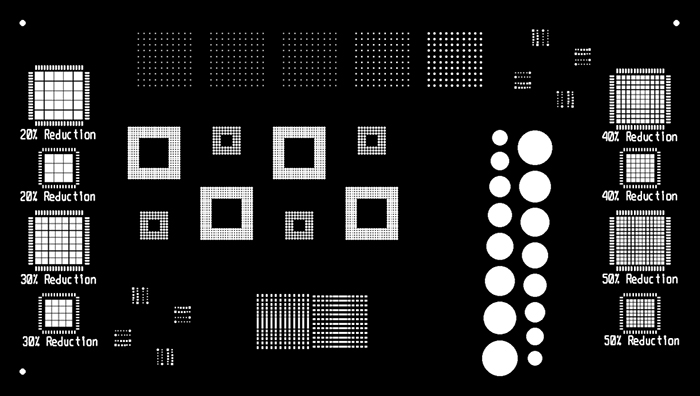
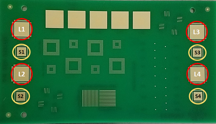
Figure 5. Second stencil design by QFN location.
Table 2. Second Stencil Design for Voiding

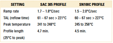
Two different reflow profiles were used, and these were specific to the solder alloys. The SAC 305 and SAC 305 90% / SN100C 10% solder pastes were run through the SAC 305 profile. The SN100C and SN100CV solder pastes were run through the SN100C profile. Both profiles were set up in a 10-zone convection reflow oven and are standard ramp to spike (RTS) linear profiles (FIGURE 6).
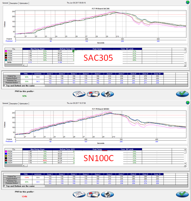
Figure 6. Ramp-to-spike profiles (top = SAC 305, bottom = SN100C).
The SAC 305 profile has a peak temperature of 241° to 248°C. The SN100C profile has a higher peak temperature of 245° to 256°C. A summary of the reflow profile parameters is shown in TABLE 3.
Table 3. Solder Alloys Studied for Voiding Potential
The x-ray system used to measure voiding was a 2D system that analyzes gray-scale to calculate voiding area. The x-ray source was set to a voltage of 70kV and a current of 400µA.
Results
Solder powder size effects on voiding. Previous work3 measured voiding by solder powder size using water-soluble solder paste B and SAC 305 Type 3, Type 4 and Type 5 solder powders (FIGURE 7). This work was expanded with no-clean solder paste C and “low-voiding” no-clean solder paste F (FIGURES 8 and 9).
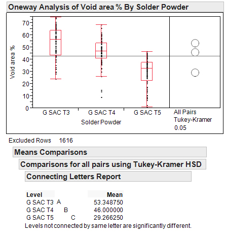
Figure 7. Voiding by SAC 305 solder powder size for solder paste B.
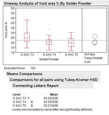
Figure 8. Voiding by SAC 305 solder powder size for solder paste C.
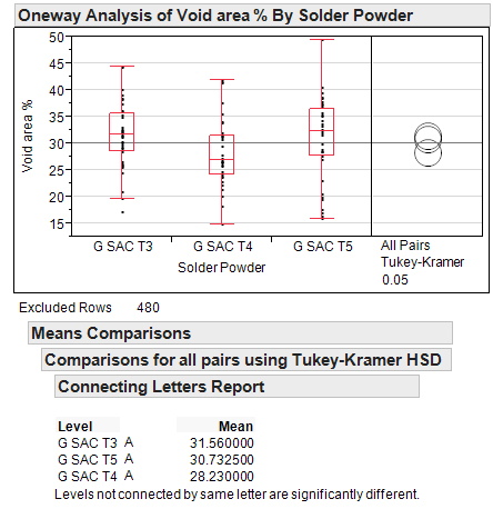
Figure 9. Voiding by SAC 305 solder powder size for solder paste F.
Solder paste B showed decreasing void area as solder powder size decreased (T3 > T4 > T5). Solder paste C also showed a decrease in void area from Type 3 to Type 4 and Type 5 solder powders. Type 4 and Type 5 solder powders showed similar voiding with solder paste C (T3 > T4 = T5). Solder paste F did not show the same trend. The void levels were similar for all three solder powder sizes for solder paste F (T3 = T4 = T5). It is clear from these results that solder powder size does affect voiding for some solder pastes, but not all solder pastes. This is similar to voiding results found by Nash and Lasky.4
Solder alloy effects. Four solder powder alloys were studied for their effects on voiding: SAC 305 Type 3, SN100C Types 3 and 4, SN100CV Type 4, and SAC 305 90% / SN100C 10% (AT mixture, Type 3). Solder paste B was used as the test vehicle for these alloys, and the results are shown in FIGURE 10.
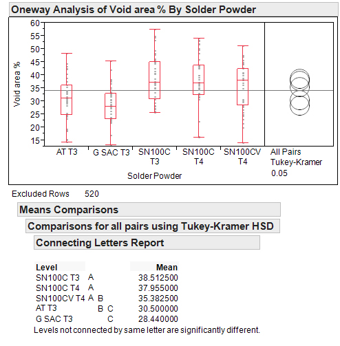
Figure 10. Voiding by solder alloy for solder paste B.
SN100C Type 3 and 4 solder powders generated the highest voiding. SN100CV alloy gave statistically similar voiding to SN100C and the AT mixture (SAC 305 90% / SN100C 10%). The AT mixture gave lower voiding than SN100C but similar voiding to SN100CV and SAC 305. SAC 305 gave lower overall voiding than SN100C and SN100CV.
The trend in voiding roughly follows the width of the melting range of the alloys. SN100C melts at one temperature and gave the highest voiding. SN100CV has a 4°C melting range and gave moderate voiding. SAC 305 has a 3°C melting range and gave low voiding. The AT mixture has a melting range of 10°C and gave low voiding. As the melting range widened, voiding tended to decrease.
Surface finish effects. Voiding was studied in previous work3 with both ENIG and OSP surface finishes and solder paste B (FIGURE 11). Voiding for ENIG and OSP surface finishes was very similar with solder paste B. This test was repeated with another water-soluble solder paste E
(FIGURE 12). Again, voiding levels were similar for both ENIG and OSP surface finishes with solder paste E. The same is not true for no-clean solder paste C (FIGURE 13). Voiding was significantly lower for ENIG surface finish than OSP surface finish with no-clean solder paste C. This result shows surface finish can affect voiding levels for certain solder pastes.
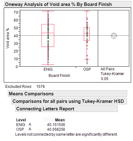
Figure 11. Voiding by surface finish for solder paste B.
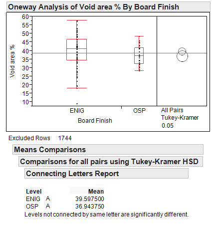
Figure 12. Voiding by surface finish for solder paste E.
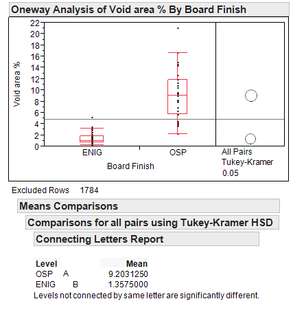
Figure 13. Voiding by surface finish for solder paste C.
Solder paste effects. It has become common for solder paste manufacturers to formulate solder pastes with the specific
intention of reducing voiding.5 A newly released “ultra-low-voiding” solder paste F was compared to an industry standard solder paste C for voiding performance (FIGURE 14). Solder paste F generated significantly lower voiding than solder paste C in this experiment. Solder paste is certainly a major factor among the potential factors that influence voiding.6 Use of a lower-voiding solder paste can reduce overall potential for voiding.
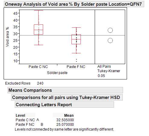
Figure 14. Voiding comparison of solder pastes C and F.
Stencil design effects. In prior work, stencil design was varied2 and voiding was studied for solder paste B (FIGURE 15). One particular stencil design (U11) was found to generate higher voiding than three other designs. In this work, four different stencil designs were tested (Figure 5), along with solder paste F. The area of solder paste coverage was varied from 50% to 80% on the QFN thermal pads. The voiding results are shown in FIGURE 16.
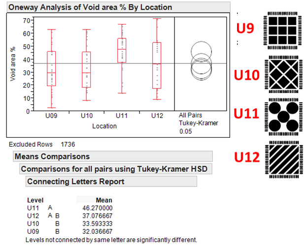
Figure 15. Voiding by stencil design for solder paste B.
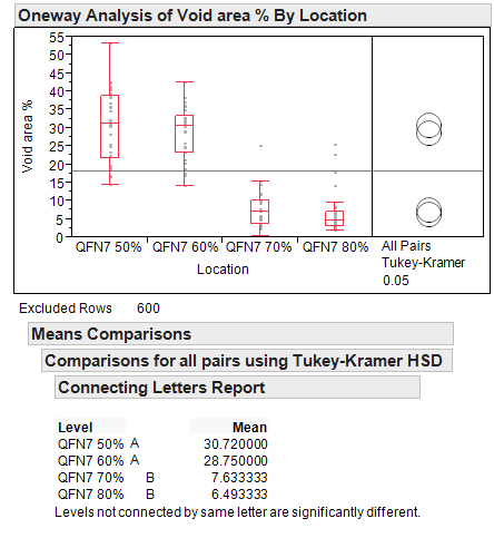
Figure 16. Voiding by stencil design for solder paste F.
It is clear 50% and 60% solder paste coverage generates much higher voiding than 70% and 80% coverage. It is worth noting that some component float and skew were seen for the 70% and 80% coverage areas. It is possible the solder paste could not fully wet the component and board pads when solder paste coverage became too low. Incomplete wetting is known to lead to void formation.7
Conclusions
What have we learned about voiding?
- Solder powder particle size affects voiding for some solder pastes. Voiding tends to decrease as solder powder size becomes smaller.
- Solder alloy affects voiding and seems to follow a trend with melting range. Wider melting ranges tend to generate lower voiding levels. Voiding could be influenced by other factors related to solder alloys not evaluated in this study.
- OSP showed higher voiding than ENIG for a no-clean lead-free solder paste tested. Two different water-soluble lead-free solder pastes showed similar voiding levels for OSP and ENIG.
- New “low-voiding” solder pastes are becoming more common. In this work, low-voiding solder paste F showed lower voiding than an industry standard solder paste C.
- Stencil design has an impact on voiding. In this study, area of printed solder paste coverage was varied. Voiding levels were much higher for 50% to 60% solder paste coverage than for 70% to 80% solder paste coverage.
Based on the results of this work, here are recommendations to help “fill the void”:
- Use of smaller solder powder sizes can reduce voiding with certain types of solder paste.
- Use of specific solder alloys may help mitigate voiding.
- Use a solder paste that works well with the surface finish to minimize voiding.
- Use “low-voiding” solder pastes to reduce overall potential for voiding.
- Optimize stencil design for the components to permit complete wetting and gas escape routes.
Future Work
Voiding is an issue for via-in-pad board designs, regardless of solder paste used. Via plugging options and stencil designs can help mitigate this type of voiding. Work is planned on via-in-pad voiding issues and will be presented at a future technical conference.
Acknowledgments
I would like to acknowledge the contributions of my counterpart Greg Smith, who designed the stencils used in this work. I would also like to thank Andrea Motley, a summer intern, who performed much of the testing for this paper.
References
1. K. Sweatman, T. Nishimura, K. Sugimoto and A. Kita, “Controlling Voiding Mechanisms in the Reflow Soldering Process,” IPC Apex Expo, March 2016.
2. T. Lentz and G. Smith, “Fill the Void,” SMTA International, September 2016.
3. T. Lentz, P. Chonis and J.B. Byers, “Fill the Void II: An Investigation into Methods of Reducing Voiding,” IPC Apex Expo, February 2017.
4. C. Nash and R. Lasky, Ph.D., “Minimizing Voiding in SMT Assembly of BTCs,” SMTA International, September 2016.
5. L. Ma, F. Chen and N. Lee, Ph.D., “Ultra Low-Voiding, Halogen-Free, No-Clean, Lead-Free Solder Paste for Large Pads,” SMTA International, September 2016.
6. L. Ma, F. Chen and N. Lee, Ph.D., “Ultra Low-Voiding, Halogen-Free, No-Clean, Lead-Free Solder Paste for Large Pads,” IPC Apex Expo, February 2017.
7. B. Sandy-Smith, “Voiding Performance with Solder Pastes Containing Modified SAC Alloys for Automotive Applications in Bottom Terminated Component Assemblies,” IPC Apex Expo, February 2017.
Ed.: This article was first presented at SMTA International in October 2017 and is published here with permission of the author.
is chemist/field application engineer at FCT Assembly (fctassembly.com); tlentz@fctassembly.com.


