Improving Fabrication Yields
How the CAM engineer can make the difference.
Embedded in fabrication planning is calculating panel size, checking layer stackup information, reviewing expected yields, reviewing board construction and verifying impedance control calculations.
Typical panel sizes are 9 x 12˝, 12 x 18˝, 18 x 24˝, or 18 x 36˝. A number of factors need to be considered when calculating panel size. For instance, consider a small board of 25˝2. A relatively high number of this small board can be panelized in an 18 x 24˝ panel. But board complexity and density, or such factors as high-speed signals, trace thicknesses, or controlled impedance, could favor a 9 x 12˝ panel.
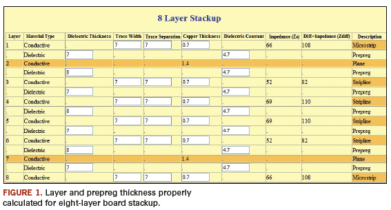
Stackup calculation is another planning aspect. Figure 1 shows the construction of an eight-layer board stackup with properly calculated layer and prepreg thickness. Stackup depends on the number of layers, the construction design, and the prepregs. It’s important to understand how a PCB’s layers and prepregs are constructed because they come in different amounts of copper. They also come in different thicknesses, and depending on the number of layers, board construction can change, thereby either increasing or decreasing yield.

When impedance control calculations are involved, the CAM engineer should work closely with design engineers.
Innerlayer registration. Buried capacitance (or buried resistance) is a technique sometimes applied when there is no available surface real estate to place passive components or when placing them creates noise that cannot be suppressed. In such instances, innerlayer registration requires special attention. Extremely thin prepregs (in the range of 0.002˝) demand careful handling. It is very hard to align such thin prepreg material during internal layer lamination process.
CAM engineers must ensure internal layers are properly registered, taking into account potential shifts occurring in layer construction. Fine-pitch devices require careful attention because they use extremely thin traces, thus posing impedance calculation issues. AOI is a solution here. AOI can check for internal shorts or opens before or even after boards are laminated, although changes after the latter are expensive.
If mechanical drills are used for holes in the range of 0.006˝ to 0.009˝, extra-fine drill bits with extremely tight tolerances are required. Also, routing issues come into play when components are stacked toward the board edge. If the tolerances are not tight, the drilled holes can encroach into other areas, possibly damaging traces or pads.
A word of caution. It’s not a good idea to stretch the technology. Put another way, a fabricator may not have the most advanced technology in-house. If outdated equipment is pushed beyond its limits, fabrication yields may decrease. For example, an older mechanical drill may be designed to form 0.008˝ holes, but the design calls for 0.005˝ holes. The situation may call for a laser drill, as mechanical drills lack the precise tolerance needed, which could result in overly large or wide drilled holes. Cutting into other traces or creating opens or shorts jeopardizes board integrity. It’s better to match the technology to the level of board fabrication complexity.
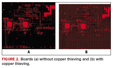
Manufacturing practices. In board fabrication, good manufacturing practices go hand-in-hand with advanced technologies. Those preventive maintenance practices are synonymous with maintaining and properly and frequently calibrating fabrication equipment and systems. Precise calibrations are critical for ensuring proper drilling, routing, etching, and maintaining plating and etching chemistries. Another best practice to increase fabrication yield is copper thieving. It is used to balance the copper on the PCB surface, making the etching uniform and thereby reducing the chances of board warpage (Figure 2).

First-article creation and inspection represents yet another important aspect that can tremendously improve fabrication yields. At the beginning stage, after CAM planning is done, the fabricator should create a first article by aligning all the drill holes with through-hole pads, creating drilling and routing files, and checking power and ground planes for opens and shorts. A first-article board is then built to make sure all the critical factors are properly addressed.
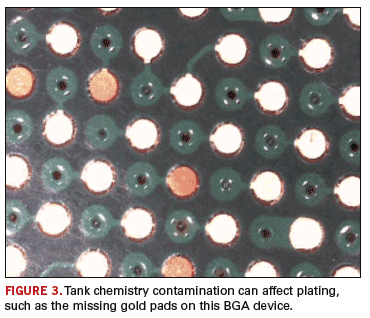
Chemistries. A fabricator has an assortment of chemical tanks. Maintaining effective chemistry balance is vital in etching tanks and plating lines. It is always a good idea for a fabricator to maintain an in-house chemical laboratory that can frequently monitor the chemistry in each bath. Some types of chemistry require checking every day – others every two to three days, depending on their processes and critical elements constituting those chemistries. Maintaining proper chemistries can boost board yield. If tank chemistries are not monitored properly, it can cause contamination, thereby creating uneven plating (Figure 3).

Finally, advanced fabrication equipment technology and preventive maintenance are inextricably intertwined; one isn’t effective without the other. Proper calibrations and maintenance are demanded when fabricators perform special builds such as countersink holes, back or stub drilling, or sequential laminations.
Zulki Khan is president and founder of Nexlogic Technologies (nexlogic.com); zk@nexlogic.com.


