Using Automated 3D X-Ray Inspection to Detect BTC Defects
Detecting marginal joints and other solder-related defects on high-temperature thermal pads.
Bottom-termination components (BTC), such as QFNs, are becoming more common in PCB assemblies. These components are characterized by hidden solder joints. How are defects on hidden DFN joints detected? Certainly, insufficient solder joints on BTCs cannot be detected by manual visual inspection. Nor can this type of defect be detected by automated optical inspection; the joint is hidden by the component body. Defects such as insufficients are often referred to as “marginal” defects because there is likely enough solder present to make contact between the termination on the bottom-side of the component and the board pad for the component to pass in-circuit and functional test. Should the board be subjected to shock or vibration, however, there is a good chance this solder connection will fracture, leading to an open connection.
QFN solder joint defects are very difficult to detect using 2D x-ray. Often, under 2D x-ray, a defective solder joint does not look very different from a good solder joint. 3D AXI looks at the solder joint profile, takes measurements and compares these measurements to that of a good solder joint. If the joint under inspection is defective, its profile measurements will differ from those of a good solder joint (Figure 1).
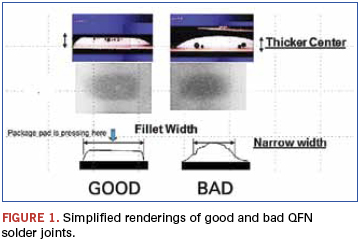
The good joint (left) shows the solder paste has “wetted” and the part collapsed on the pad, creating a wide, thin solder joint. On the right, there is no wetting, resulting in an open joint. The characteristics of an open joint are a higher solder center thickness measurement, a narrower center width, and a smaller slope of the outer edges of the joint. 3D AXI can take measurements of these various characteristics of good QFN solder joints and set them as standard values for use in the testing of components on subsequent boards.
Figures 2 and 3 show open and marginal joints detected with 3D AXI. Figure 2 shows poor wetting of solder and an insufficient deposit of solder paste, resulting in a smaller solder joint. As stated, marginal solder joints will likely pass ICT and FCT because there is a slight solder connection between the PCB pad and component, but ultimately may fail in the field.
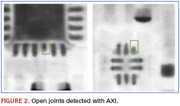
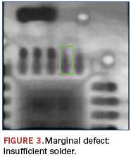
Figure 4 shows a short detected by 3D AXI. Note that in this case, ICT might detect this defect. More often, the time required to troubleshoot at ICT to locate the actual defect location is much longer, leading to increased labor costs. 3D AXI pinpoints the exact location of the defect for repair or replacement.
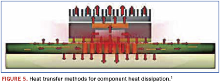
Field-effect-transistors (FET) are high-power devices, which, due to their high computing power, generate high levels of heat. It is necessary for designers to ensure adequate means of dissipating this heat. Traditionally, before the rise in miniaturization, designers often relied on heatsinks or heat spreaders placed on top of the device to dissipate this heat (Figure 5). For smaller, low-profile consumer products, designers are eliminating heatsinks and are relying instead on thermal pads to dissipate heat. 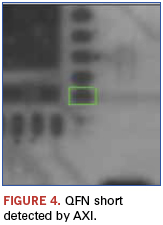
FET devices, if not attached to the board with sufficient solder, can overheat and result in one of two scenarios: First, the overheated device could have its electrical characteristics altered, reducing its reliability and ultimately resulting in component failure. This failure may not occur immediately, but at a later time. Second, and much more serious, the component temperature could rise to such an extreme that an exothermic reaction could occur, not only immediately damaging the component, but sometimes damaging the actual assembly. In general, the higher the temperature to which a component is exposed, the shorter its life.2
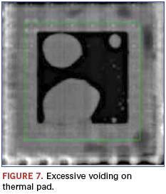
The most common defects for these thermal pads are opens, whereby solder joints appear grainy under x-ray (Figure 6B) or demonstrate excessive voiding (Figure 7). Either defect on some thermal pads can create a localized area of high thermal resistance. Most 3D AXI can reliably detect these defects.
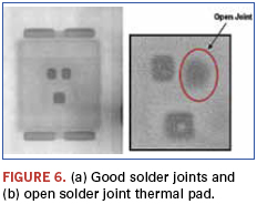
For detecting cold solder joints, 3D AXI again looks at the slope of the joint. A cold solder joint will have a much smaller slope than that of a good solder joint.
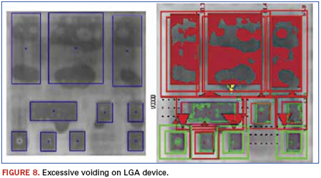
For detecting voids, 3D AXI looks at the gray level of each pixel on the pad and compares it to a nominal gray level value. If the delta between the nominal value and measured value is greater than a certain amount, the pixel is considered to be part of a void. The AXI then compares the void area to the pad area to determine the void percent. Figure 8 shows a land grid array (LGA) with excessive voiding on three pads. Notice how 3D AXI highlights in green or red each pixel with a gray level delta in excess of the allowable value. For pads for which the summation of these highlighted pixels is greater than the maximum allowable “void percent” set by the user, the pixels appear in red, signifying a failed joint.
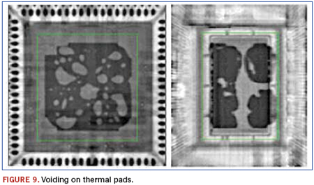
Most mosfet manufacturers specify maximum allowable void percentages, generally 25% to 30% of the pad area. A good reliable solder connection between a component’s thermal pad and the PCB is critical to long-term survival of these high-power devices. It’s critical to inspect the solder joint integrity of the thermal pads before the board is powered up (either at FT or repeatedly by the end-user). If defects are not detected and repaired before full power up, there will most likely be some component degradation or more catastrophic damage. Figure 9 shows examples of thermal pad void defects detected by 3D AXI.
Ball grid arrays are another type of hidden joint device commonly used on PCBs. The most common types of defects found during 3D AXI are insufficient solder, opens, voids, misalignment and shorts. To detect these defects, 3D AXI looks at the diameter and gray level of each joint at multiple slices (Figure 10) and compares the measurements collected with standard or nominal values set by the user. These nominal values are determined using what is referred to as a golden board, or a board with no defects. The golden board is tested and nominal values automatically calculated for use in testing of all subsequent boards. 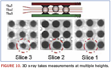
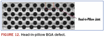
3D x-ray has an advantage over 2D in that it can take up to five slices for the various devices. This is especially important for BGA devices because some defects, such as head-in-pillow (HiP) (Figures 11 and 12) occur at the board level. Therefore, it is important a diameter measurement is taken close to the board surface, where the HiP joint often exhibits a smaller diameter or the ball is slightly offset from the center. 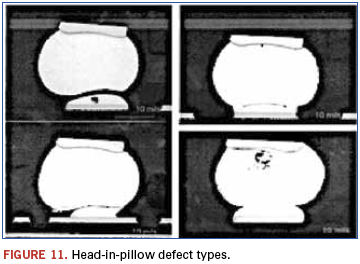
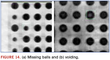
Of the various types of BGA defect types detected using AXI (Figures 13 and 14), especially interesting is Figure 13A, which shows a foreign particle (possibly a clipped PTH lead) trapped beneath a BGA. This type of defect can easily turn into a short as the particle moves beneath the device; however, due to its movement, it may not be easily detected at ICT. 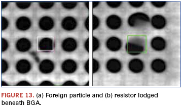
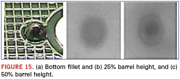
Insufficient barrel fills can also easily go undetected and lead to reliability problems. Often there is a very good fillet visible at the bottom side of the board. But, especially for power and ground pins, solder often does not flow up the barrel adequately during wave soldering. Because 3D AXI can take multiple slices, the user can specify the z height for AXI inspection. For example, IPC-A-610E specifies barrel fill up to at least 75% for signal pins.3 Figure 15A shows a joint with a perfectly good visible fillet on the bottom-side. A measurement (slice) taken at 25% up from the bottom (Figure 15B) continues to show good solder fill. However, at 50% up into the barrel (Figure 15C), there is no solder present. The only object visible in the x-ray image is the device lead.
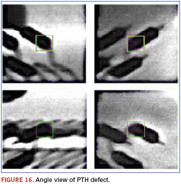
To help during dispositioning of PTH defects, some AXI systems show angle views of the defective components at the AXI repair station (Figure 16). This assists in confirming that defect is a valid call. This angle view feature minimizes incorrect dispositioning of defects; i.e., it reduces the number of “escapes” of true insufficient solder defects.
Consumer product manufacturers are finding it necessary to incorporate automated 3D x-ray inspection (AXI). 3D AXI can detect defects on hidden joints, and can be placed inline, making it feasible for volume manufacturers.
References
1. Arlon, Materials for Electronics Division (MED).
2. E.A. Amerasekera and F.N. Najim, “Failure Mechanisms of Semiconductor Devices,” John Wiley, 1997.
3. IPC-A-610E, Acceptability of Electronic Assemblies, April 2010.
Acknowledgments
Thanks to Andy Pascual of Jabil.
Ed.: This article was first presented at the International Conference on Soldering & Reliability in May 2011 and is reprinted with permission of the authors.
Barbara Koczera handles pre/post sales support at Test Research USA (tri.com.tw), and An Qi Zhao is with Flextronics (flextronics.com); barbara@tri.com.tw.


