Interconnects Drive Heterogeneous Assembly and Substrate Options
Is the time for MCMs or so-called “hybrid assemblies” finally at hand?
Product designers are turning to mixing and matching component configurations so their products can achieve the smallest form factor and highest performance possible. Our accepted term for this mashup is called heterogeneous assembly.
Heterogeneous is the latest branding effort to promote the assembly of dissimilar electronic components. In the past these could be called multichip modules, 2.5-D, 3-D and – really going back – “hybrid” assemblies. How the selected components are interconnected drives how they are assembled and what substrate materials will work.
As with any new set of tools, it’s necessary for users, especially designers, to know what they can and can’t use easily, economically or reliably. It’s equally important for anyone wanting a heterogeneous assembly to understand the consequences resulting from the interconnections and materials chosen, and to realize that currently they are available from a limited base of capable assemblers.
Interconnection Options
The same interconnection processes used for decades are still the main choices. However, it’s no longer a simple case of wire bonding or soldering a part to a substrate, as the materials and components being interconnected have changed. Now, designers are specifying die-on-die, package-on-package, and die-on-package, and using solder balls, copper pads and pillars, gold leads, and so on. With these combinations, we need to add thermocompression bonding, laser reflow, vacuum reflow, and maybe even vapor phase soldering to the tools necessary for successful assembly.
FIGURE 1 shows a simplified assembly flow of the most common heterogeneous assembly process often starts with SMT. Some common packaging methods used for heterogeneous devices include:
- Die stacking with and without spacers
- Flip-chip
- 2.5-D integration using silicon interposer
- 3-D integration using through-silicon vias (TSV)
- System-in-package (SIP) utilizing multiple interconnected die and parts.

Figure 1. Overall heterogeneous assembly process.
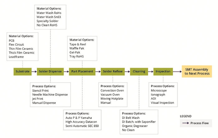
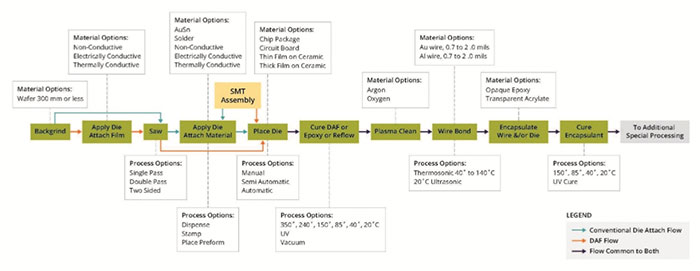
With complex heterogeneous devices, it is not uncommon to need as many as 50 additional steps for assembly of a single device or product, and sometimes more. FIGURE 2 illustrates some of these additional subassembly steps. FIGURE 3 details the process when subassembly is used as a platform on which die processed from semiconductor wafers are attached and connected.

Figure 2. Surface mount process options.

Figure 3. Wafer processing through die attach and wirebond flow.
While the assembly steps and packaging methods shown in Figures 2 and 3 are a good starting point, heterogeneous integration often requires combining these conventional processes with specialized processes specific to the device. For example, while most electronics products are built on printed circuit boards, many heterogeneously integrated devices are physically small and thus must utilize an equally small circuit board or other type of substrate.
Substrate types include thick-film ceramics, thin-film ceramics, silicon, glass, or flex circuits. Some of these are panelized, while others are provided as individual parts. Because processing multiple devices in parallel is a good way to reduce cost, substrates that are not panelized can often be placed in fixtures that enable parallel processing and minimize handling, or enable mechanizing of handling, and thus minimize damage during processing.
Complex Design
As with most products, good performance and low cost start with and are dominated by good design. Heterogeneous integration makes the design function much more complex than is typical for electronic products because many parameters can impact performance. Additional design issues include:
- Design software. Especially functional simulation as is done for electronics utilizing SPICE models. Models of that level of sophistication do not exist for most heterogeneous, integrated products. Thermal and RF analysis is still being enhanced. Designing heterogeneous devices often requires the use of SolidWorks, 3-D design and simulation software, as well as classic electronic design software, and usually some specialized custom software.
- The lack of good data on materials and their properties. As an example, considering an implantable medical device must cause no harm when it encounters human tissue, it’s obvious why having good data on materials used in the device is essential. Fluids or organic materials may become contaminated by materials in the implantable device or may cause the device to deteriorate in some manner. Designing around the relevant, detrimental phenomena is difficult, even when material properties are well known. Optical devices also require extreme mechanical stability to avoid unwanted effects over the life of a product. Optical attenuation results, especially from thermal- and stress-induced motion, but also from yellowing, crazing, etc. RF properties of many materials (the dielectric constant and loss tangent) vary with frequency, water content, etc., in ways that are poorly documented.
- Availability of components and materials. Sourcing heterogeneous components is complex due to the wide variety of parts that must be sourced. A wider variety increases the number of vendors needed, the length of the resulting supply chain, the cost resulting from margin stack of multiple vendors, and the need for some level of part traceability and compliance with the variety of quality requirements. Compatible second-source components are fleeting.
Developing and managing the supply chain should begin with design and proceed in parallel. Good design is of no value if the parts, materials and equipment required are not available in a timely manner with acceptable cost and quality. - Cost. One of the most popular trends – the requirement to reduce the size of heterogeneous devices to make them more convenient to use – often minimizes power consumption and costs by utilizing a small amount of material. However, cost is raised by the increased number of parts, the complexity of the supply chain, the number of assembly processes and the increased precision required by the small size.
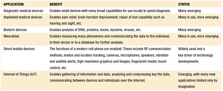
Despite the design challenges, many applications are enabled with heterogeneous integration. TABLE 1 provides examples of those applications and the adoption status in today’s market.
Table 1. Applications Benefiting from Heterogeneous Integration
Rapidly Increasing Demand
The world of electronic products is continually getting smaller and more capable. New products are combining the data gathering, analysis, storage and communication capability of classic electronics with additional components that interact with the user and environment to gather primary information. Prime examples are medical devices and smart home electronics. This continues to challenge the electronic substrate and assembly world. There are limited numbers of compatible design software and capable manufacturing resources. At previous inflection points in the industry, such as SMT, industry groups gathered to help facilitate the growth of resources.1 Efforts have been initiated in the past to facilitate heterogeneous acceptance but were too early to gain traction.2
If the number of recent seminars that have focused on heterogeneous electronics is any indication of interest, the time is ripe for the industry to agree on common infrastructure.
Bibliography
1. Surface Mount Council, “Surface Mount Technology: Status Of The Technology Industry Activities and Action Plan,” August 1999, (ipc.org/4.0_Knowledge/4.1_Standards/smcstatus.pdf).
2. The 3D Business Council. Initiated by Phil Marcoux in 2012 as an initial effort to facilitate orderly standards and acceptance in the industry. The initial meeting, with over 35 attendees, spawned follow-on efforts by SEMI, IPC, IEEE, and others.
is president and CEO of Promex Industries (promex-ind.com). He has an MBA from Harvard and bachelor’s and master’s in electrical engineering from MIT. is managing director of PPM Associates; oneppm@ymail.com.


