Comparison of Aperture Designs, Solder Pastes, Nanocoatings and Print/Inspection Systems
Testing transfer efficiency and repeatability for microminiature devices down to 01005 discretes and 0.4mm BGAs.
High-reliability PCB assemblers face multiple challenges from the mainstream industry’s migration to lead-free solders. One of the major challenges is in the solder paste itself. Solder paste manufacturers have been continuously developing new lead-free solder pastes for approximately 15 years. Few, if any solder suppliers, have introduced new SnPb solder pastes however, due largely to low market demand. Even if better SnPb paste formulations were available, changing them in a mission-critical application would require a great deal of due diligence and qualification testing.
The overall approach to SMT process optimization starts at the front of the assembly line and reviews each individual process moving down the line. Therefore, the method of optimizing production of discrete sizes 01005 to 0402 (Imperial) starts with optimizing the print.
The aperture design in the process of record (POR) for these component packages is shown in FIGURE 1. It is known as the “inverted home plate,” “crown,” “bowtie” or “Pac Man” aperture design. This is a common aperture design to minimize solder paste under the terminations, and therefore the propensity for mid-chip solder balls (MCSBs). It was identified in 20041 as the optimum aperture design to limit MCSBs with SnPb solder paste and 5 or 6 mil foils. At the time of the study, 0402 packages were the smallest available to test. Today they are mainstream, and many lessons have been learned. The acute angles in the corners, although radial, are still very tight on 0402s and can create release issues for solder paste. The release issues can then lead to defect modes such as tombstoning, skews or non-wets, especially if placement is slightly off-target.
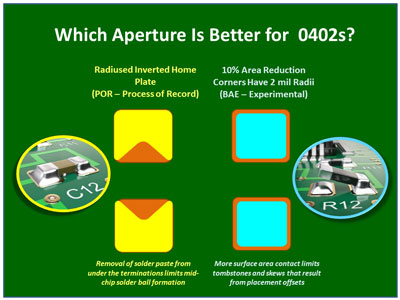
Figure 1. Aperture designs tested for 0402 (1005M).
This experiment examines the printability of the POR aperture design with a simple rectangular one with a 10% area reduction for 0402s. Printability of the two aperture types are compared using transfer efficiency and coefficient of variation as output variables, on the assembler’s production line using its qualified solder paste.
The next experiment does the same thing with the same solder paste, but in a laboratory environment as opposed to a production line, and uses an earlier model SPI machine from the same manufacturer.
The final test also takes place in the laboratory, comparing a slightly newer version of SnPb solder paste with a SnPb paste made with a “backwards-compatible” flux. The term backwards-compatible indicates the flux was designed for higher-temperature, lead-free products, but works well with SnPb solder powder and does not present electrochemical reliability concerns after a cooler, SnPb reflow cycle.
The assembler cannot bring the solder paste in-house to test, so the study looks for correlations in SPI readings on the control paste to determine if the experimental product will make enough impact on print quality to invest in the qualification process.
Experimental Design
Test vehicle. The test used the SMTA miniaturization test vehicle (FIGURE 2). It contains numerous miniaturized components; the ones primarily studied in this test are:
- Ten 0.5mm BGAs
- Nine 0.4mm BGAs
- Eight blocks of 01005 (0402M) components, 100 each
- Eight blocks of 0201 (0603M) components, 100 each
- Eight blocks of 0402 (1005M) components, 100 each
Sample sizes for each 10-print test were:
- 2880 0.5mm BGA deposits
- 5,580 0.4mm BGA deposits
- 16,000 0402 (1005M) deposits
- 16,000 0201 (0603M) deposits
- 16,000 01005 (0402M) deposits
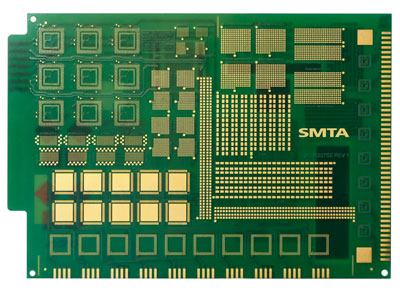
Figure 2. Test PCB.2, 3
Stencils. Six of each stencil thickness were tested, configured as described in TABLE 1. All stencils were laser-cut from fine-grain stainless steel and mounted at standard tension (~34N/cm). Six each were produced in 4 and 5 mil thicknesses. Three of each thickness had the POR aperture design (per IPC-75254), and three had the experimental aperture design (abbreviated BAE in the data reduction). Each set of three stencils was then subdivided by coating. One had no coating (naked), one had ceramic coating (cured on), and one had a phosphonate coating (wipe-on).
Table 1. Stencils Used in Test
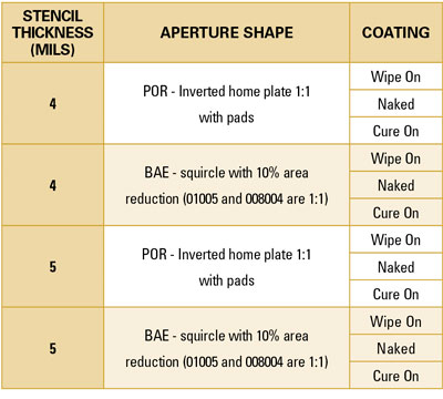
Based on experience with variability on the 0402 POR apertures and the sizes of 0201 and 01005 apertures, inverted home plate designs were not attempted for the smaller devices. Both the POR and BAE stencils used the same aperture sizes for 0201 and 01005 components. They are shown in TABLE 2.
Table 2. Aperture and Pad Sizes for Miniaturized Discretes

Test execution. Each print test consisted of 10 prints, with a wipe between each print. The assembly line used:
- Vac, wet, oscillate
- Vac, dry, oscillate
- Dry, vac, oscillate
The laboratory used a dry/vac, dry/vac between prints.
The assembler’s production floor used a new EKRA Serio 4000 stencil printer certified by Cetaq5 and a Koh Young Aspire 3 with four projectors and a 12Mp camera at 15μm resolution.
The laboratory used a new MPM Edison 2 stencil printer that had been recently certified via Cetaq, and a Koh Young 8030, a two-projector system with a 4Mp camera at 15μm resolution. It was later upgraded to an Aspire 3 with four projectors and a 12Mp camera at 10μm resolution between the incumbent paste print tests and the followup ones.
Both facilities used handheld ultrasonic stencil cleaners6 to ensure the best possible removal of residual solder paste from the apertures before transferring stencils to the other facility. Also, stencils were cleaned with ultrasonic cleaning systems upon arrival from the stencil manufacturer.
Note that it is important to clean new stencils before they are put into service to remove any residual burrs or contaminants from the cutting process. Stencils with cured-on coatings do not need to be cleaned upon arrival because they receive a thorough cleaning before the coating is applied. In fact, they should not be exposed to any harsh flux-dissolving solvents for 72 hr. after their cure, to permit complete cure of the coating.
Both the control and experimental solder pastes were Type 3, SnPb, no-clean products. Because the boards in this test were not populated, flat plates were used for tooling support on the production floor. Custom tooling plates were used in the laboratory. Again, because nothing was populated, the PCB support – a key element of the printing process – was excellent regardless of facility.
The production facility used metal squeegees mounted at 65° angles, and the laboratory used surgical steel squeegees mounted at 60° angles.
Data analysis. Data were output from the SPI machines into comma-separated files and opened and saved in Microsoft Excel format. In Excel, columns were added for:
- Stencil thickness (4 or 5)
- Aperture design (POR or BAE)
- Stencil coating (naked, cured-on or wipe-on)
- Solder paste (control or experimental)
- Location – Nashua, NH, or Hopkinton, MA.
Each facility produced 12 SPI files with 187,000 lines of data for each solder paste.
Results
This section contains detailed statistical results from the tests. For an overview of the findings, see the Discussion and Conclusions sections.
Key findings. The purpose of the study was to answer specific questions about process changes before implementing any on high-reliability products, especially those currently in production. Questions included:
- What is the impact of migrating from 5 mil foils to 4 mil foils?
- Would different aperture designs improve the repeatability of the print process?
- What is the smallest device we can repeatably print with the current solder paste formulation?
- Would qualifying a new solder paste provide enough quality and cost improvement to justify the effort?
Foil thickness. Neither foil thickness could adequately print 01005s with the production solder paste on the production line. For both foil thicknesses and all surface treatments, coefficients of variation (CVs) ranged from 25 to 45%. The CV is simply the standard deviation divided by the mean, expressed as a percent. Typically, less than 10% is preferred, 10 to 15% is considered acceptable or marginal, and greater than 15% is considered unacceptable. These features were not expected to print well, given their area ratios and the older, Type 3 solder paste.
The 0201s showed good capability for all stencil types. CVs ranged from 5.8 to 7.0, all in the preferred range. The best performer was the cured-on coating. In the boxplots (FIGURE 3 and 4), the apertures labeled BAE are the experimental (short for BAE modifications), and the POR are the current process of record that reflects the current aperture library.
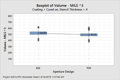
Figure 3. Boxplot and statistics for 0201 prints with a 4 mil foil and cured-on coating.
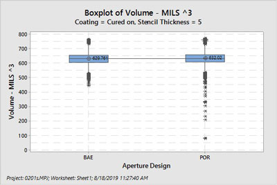
Figure 4. Boxplot and statistics for 0201 prints with a 5 mil foil and cured-on coating.
The volumes are relatively the same between the BAE and POR apertures. They should be, because in the case of 0201s, they are the same.
The 4 mil foil prints a much tighter distribution than the 5 mil foil. The 5 mil foil also tends to produce more insufficients (lower area ratio). The 5 mil foil deposits a mean volume of 630 mil3, whereas the 4 mil foil deposits approximately 500 mil3. The roughly 20% reduction in solder volume is not expected to impact solder joint integrity, as the 500 mil3 average is still typical for the package type. The reduction in variation – especially the limiting of insufficient deposits that cause tombstone, skew and non-wet defects – should improve end-of line quality. A 4 mil foil is preferred for 0201s for higher quality output.
Aperture designs. Two different aperture designs were tested on two different component types. For 0402 components, the POR aperture is the radiused inverted home plate, and the BAE aperture is a rectangle with radiused corners, also known as the “squircle.” The corner radii are 2 mil; the radii help prevent solder paste buildup in the aperture corners. For the 0.5mm BGA components, the POR aperture is a circle at 1:1 with the pad (10 mil), and the BAE aperture is a squircle the same size with 2 mil radii.
Radiused rectangle vs. inverted homeplate on 0402s. FIGURES 5 and 6 show the boxplots for 4 and 5 mil stencils with the cured-on coating. Both aperture designs on both stencil thicknesses showed good capability, with CVs well below 10%. Both aperture designs showed similar mean volumes on their respective stencil thicknesses, despite having different geometries. The reduction of volume of approximately 20% when thinning the stencil 20%, with no impact on variation, indicates area ratio is not a factor on the 0402s.
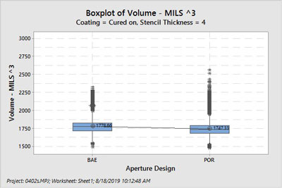
Figure 5. Boxplot and statistics for 0402 prints with a 4 mil foil and cured-on coating.
Either stencil thickness or aperture design appears equally viable from a print capability perspective. Therefore, moving to a POR aperture or 4 mil foil will not negatively impact print quality, and merits investigation into its effects on end-of-line yield, particularly with respect to the production of tombstone/skew vs. MCSB defects.
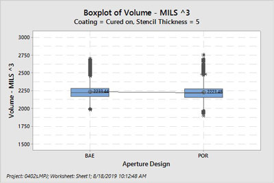
Figure 6. Boxplot and statistics for 0402 prints with a 5 mil foil and cured-on coating.
Circle vs. radiused square for BGAs. In the case of the 0.5mm BGAs, the circular aperture has a 10 mil diameter, and the squircle aperture also has a 10 mil side length, with 2 mil radii. Data were only analyzed for the 4 mil foil. If the 4 mil foil showed good capability, the 5 mil would have been analyzed. Data for the 4 mil foil with cured-on coating are shown in FIGURE 7. The circular (POR) aperture produced higher volumes, with less variation, but more outliers than the squircle (BAE) aperture; however, both have unacceptable CVs.
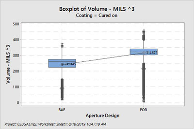
Figure 7. Boxplot and statistics for 0.5mm BGA prints with a 4 mil foil and cured-on coating.
Previous studies7,8 have shown typical 0.5mm BGA volumes in the 300 to 350 mil3 range for newer solder paste formulations. If the variations in these datasets were acceptable, the larger volume would likely be preferred. However, no realistic conclusions regarding volume and variation can be made with CVs over 15%.
The 0.5mm BGA print process is currently in place in production using POR apertures. Based on these test data, it is recommended to maintain the POR apertures while investigating other ways to improve print performance. Given the production process already uses the best-performing stencil technology, and best-in-class tooling and squeegee blades, and the printers are certified by a third party, the remaining option is to investigate the performance of newer solder paste formulations.
The 0.4mm BGAs showed complete incapability on the 4 mil foils, with CVs upward of 50% for cured-on coating, 60% for wipe-on coating and 80% for no coating. No inferences or conclusions can be drawn based on this dataset.
For reference, the POR aperture on the 0.4mm BGAs is an 8 mil circle; the BAE experimental is a 7.5 mil squircle with 2 mil radii on the corners.
Coating comparison. FIGURE 8 shows the main effects plot for volume for 0402 components. The trends shown for the 0402s are mimicked throughout the results for all datasets. The main driver for volume differences is foil thickness. Secondary to that, cured-on coatings showed higher volumes than naked stencils or wipe-on coatings, in that order. Not shown in the main effects plot are the variations of each coating. Review of all the data shows the cured-on coatings produced lower CVs than the wipe-on coatings or naked stencils, in that order.
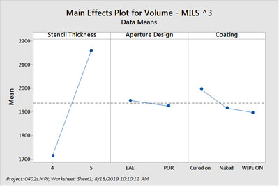
Figure 8. Main effects plot for volume on 0402s on production line.
These test results showed the print process is robust down to 0201 components, using the current equipment and solder paste. It also shows that 4 mil foils are better than 5 mil foils for this package size, because the 5 mil foils tend to produce more insufficient deposits. The 0.5mm BGAs were borderline marginal at best using the 4 mil foil with cured-on coating. They showed lower-than-expected volumes and 15% CV.
Note the population density of this PCB puts more demands on the solder paste than would a typical production PCB. A print process considered borderline on this PCB layout will likely perform better on less densely populated production boards with fewer apertures and less fine-feature component types.
Will moving to a newer formulation improve the process? Qualifying a new solder paste requires tremendous effort for any PCB assembler, let alone a high-reliability one. When considering undertaking such a substantial mission, it is important to understand if it is worth it.
To understand if a newer formulation SnPb solder paste will afford a wider process window, sample tests were run in a nearby laboratory. First, the current production solder paste was processed, then the newer products. The strongest data sets, i.e., 0201, 0402 and 0.5mm BGA apertures with cured-on coating, were compared. These tests used the same SnPb solder paste as the assembler.
FIGURES 9 and 10 show the data for the 0201s from the laboratory for comparison with data in Figures 3 and 4 generated on the assembler’s production line. The assembly line and laboratory both produced prints with CVs of approximately 6%. The volume readings on the line were higher than those in the lab. This could possibly be due to the difference in SPI machines or the difference in printers. As with the previous 0201 data, the volumes are similar because the apertures are similar.
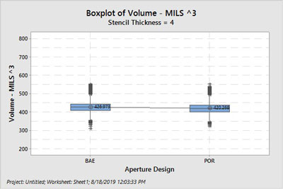
Figure 9. Boxplot and statistics for 0201 components printed with a 4 mil foil in laboratory.
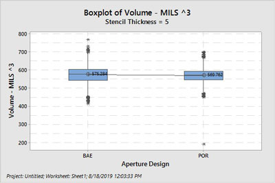
Figure 10. Boxplot and statistics for 0201 components printed with a 5 mil foil in laboratory.
FIGURES 11 and 12 show the data for the 0402s from the laboratory, for comparison with data in Figures 5 and 6 generated on the assembler’s production line. As with the 0201s, the CVs of the two processes are very close. And again, the mean of the volumes is lower for the lab than the assembly line.
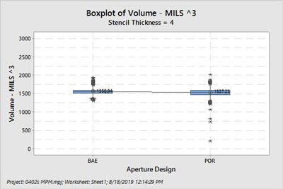
Figure 11. Boxplot and statistics for 0402 components printed with a 4 mil foil in laboratory.
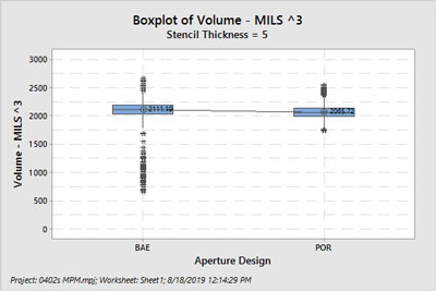
Figure 12. Boxplot and statistics for 0402 components printed with a 5 mil foil in laboratory.
The 0.5mm BGA, the finest feature to be compared, showed far less variation in the laboratory than on the assembly line. CVs for both aperture designs were acceptable. However, the distribution is much tighter for the BAE aperture (squircle) than for the POR one (round).
Considering this a viable dataset based on its CV of ~10%, the BAE aperture (squircle) is strongly preferred. Similar to the assembly line tests, it has fewer outliers than the POR, which produces many more insufficients. Also similar to the assembly line tests, the POR averages higher volumes. Similar to the comparisons of the 0201s and 0402s, the average volumes measured in the lab were lower than those measured on the line.
In an overall comparison of the datasets for 0402, 0201 and 0.5mm BGA, the assembly line readings were consistently higher. The variations however were consistent, as were the main effects. A direct statistical correlation cannot be established, but the trends are consistent.
Next, a follow-up run with two potential replacement solder pastes were printed in the laboratory using the same stencils with cured-on coatings. Because the 0.5mm BGA and 0201s printed better with a 4 mil foil, and the foil thickness had no impact on print quality for 0402s, only the 4 mil foils were print tested.
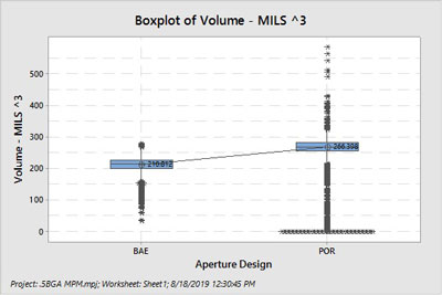
Figure 13. Boxplot and statistics for 0.5mm BGA components printed with a 4 mil foil in laboratory.
Newer SnPb or backwards-compatible Pb-free flux with SnPb powder? Two solder paste “upgrade” options are available to the assembler:
- Investigate a newer formulation SnPb solder paste that is well known as an excellent printing product.
- Investigate a formulation that was developed for Pb-free solders but provides the needed electrochemical reliability when used with SnPb alloy in SnPb reflow profiles.
Both were print tested in the laboratory. The results are shown in FIGURES 14 to 16.
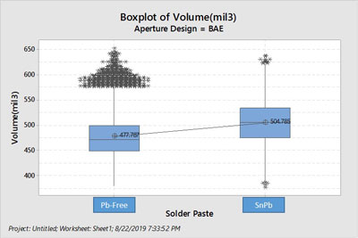
Figure 14. Boxplot and statistics for 0201 volumes with newer solder pastes.
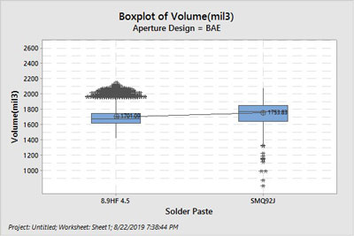
Figure 15. Boxplot and statistics for 0402 volumes with newer solder pastes.
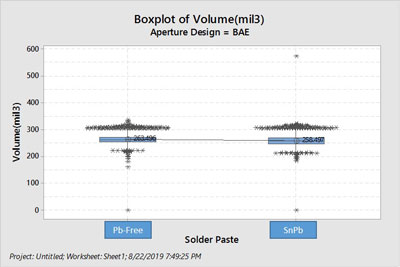
Figure 16. Boxplot and statistics for 0.5mm BGA volumes with newer solder pastes.
All the aperture sizes tested (0.4mm BGA and 01005 not shown) demonstrated similar trends in the data: very tight distributions with an unusually high number of outliers. Comparing the 0.5mm BGA print volumes for BAE apertures shown in Figure 16 against those in Figures 7 and 13 exemplifies the differences.
The follow-up dataset printed in the laboratory – the newer SnPb and Pb-free/backwards-compatible solder pastes – was on a new lot of test boards. Subsequent investigation of the boards revealed the solder mask was higher than the pads, creating contact and gasketing problems between the stencil and pad. This provides a highly plausible explanation for the atypical distribution of the volume data. An example of solder mask higher than the PCB pad is shown in FIGURE 17.
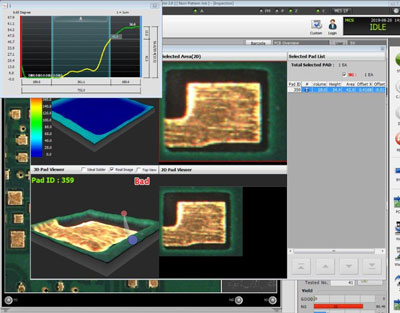
Figure 17. SPI screenshot showing solder mask taller than PCB pad, which prevents proper gasketing of the stencil to the board.
Additionally, between the original print tests and the final set on the newer solder pastes, the SPI in the laboratory was upgraded to a Koh Young Aspire 3 with 10μm resolution and four 12MP cameras. It is faster and more accurate than the earlier model used in the main part of the laboratory study. There is little likelihood that the new machine contributed to the different distribution trends, however, other than measuring them more accurately than its predecessor.
The last two datasets for the newer solder pastes showed extremely good repeatability, despite the print deficit of solder mask above the pads on the second set of test PCBs.
Discussion
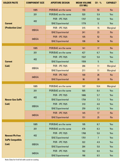
If each print process is evaluated using criteria based on CVs, where less than 10% is considered capable, 10 to 15% is considered marginal, and over 15% is considered not capable, performance can be easily categorized.
On the assembler’s line using the current SnPb solder paste, this test showed the process was completely capable of printing 0201 and 0402 components, preferably with a 4 mil nanocoated foil to help get sufficient release on the 0201s. It also showed a borderline marginal/incapable CV of 15.4% on 0.5mm BGAs with the POR aperture only, and complete incapability on smaller components. Again, it should be noted the capabilities will improve on less densely populated production PCBs, as this test layout is designed to stress solder paste.
On the laboratory line using the current SnPb solder paste, the process was also capable of 0402, 0201 and marginally capable 0.5mm BGAs (11% CV), regardless of aperture design. The volumes were slightly lower in all cases, and the CVs were much lower on the smaller apertures. The differences could be attributed to either the printer or the SPI machines.
The process improved with the newer SnPb solder paste formulation, which demonstrated good capability on 0.5mm BGAs and good/marginal on 01005s. Finally, the newest solder paste performed the best, showing good capability on all component sizes, including 0.4mm BGA and 01005, despite the handicap of excessive solder mask.
The best print performance was realized with the cured-on nanocoating, followed by the wipe-on nanocoating, with the naked stencil consistently showing the most variation. The assembler currently uses the cured-on nanocoating as the preferred finish on all its stencils.
TABLE 3 summarizes the results for a 4 mil foil with cured-on nanocoating.
Table 3. Solder Paste Print Capability
Conclusions
The information sought and gained by the test includes:
What is the impact of migrating from 5 mil foils to 4 mil foils? Reducing the stencil thickness from 5 mil to 4 mil reduces the volume on the 0402s by approximately 20% but maintains excellent repeatability and provides enough solder to form a proper joint. Reducing the thickness helps improve the 0201 process by eliminating insufficient deposits that lead to wetting problems. It also helps the 0.5 and 0.4mm BGA deposition processes in a similar fashion.
The 0.5mm and 0.4mm BGAs showed poor print performance with the incumbent solder paste on 4 mil foils and complete incapability on 5 mil foils, but fared better with the newer solder paste formulations, particularly on the 4 mil foils. The main differences between BAE and POR aperture outputs on the 0.5mm deposits were the volumes, not the repeatability, as both showed similar CVs. The two designs’ performance was almost identical on the 0.4mm deposits with the only capable solder paste (the newest).
Would different aperture designs improve the repeatability of the print process? For 0402s, the POR and BAE apertures deposit equivalent amounts of solder paste, but the BAE experimental aperture is believed to limit tombstone defects better than the POR. Because the volumes are similar, it should be easy to implement on an assembly line to see if it helps with tombstone and other wetting-related defects.
For BGAs, the POR is currently better for the 0.5mm prints, but neither aperture is acceptable for 0.4mm prints in the current process. With the newest solder paste, the 0.5mm benefited from the BAE experimental aperture, whereas the 0.4mm did not show a significant difference between the two designs.
What is the smallest device we can repeatably print with the current solder paste formulation?
Answer: 0201s. A 4 mil foil provides better quality in terms of fewer insufficient deposit volumes.
Would qualifying a new solder paste provide enough quality and cost improvement to justify the effort? Based on the findings in the laboratory, the assembler can gain a great deal of print capability by modernizing its solder paste formulation. Increases in print capability lead directly to decreases in defects, rework, scrap and lost time.
A tremendous amount of effort is required to change solder pastes, so the increase in productivity must be weighed against the investment and timed appropriately to continue the flow of new product introductions with miniaturized components. If the investment is made, the obvious choice would be to qualify the newest flux formulation in the backwards-compatible SnPb solder paste. The print performance difference is considerable and will eventually be needed as miniaturization continues.
Future Work
The stencils have been preserved to continue studying print capability on the fine features. The assembler may use them to further investigate new solder paste products to improve the assembly process. Additionally, other solder pastes may be printed in similar tests to benchmark performance among popular products.
References
1. C. Shea and R. Pandher, “Optimizing Stencil Design for Lead-Free Processing,” SMTA International Proceedings, October 2004.
2. D. Dixon, et al, “Development of a Solder Paste Test Vehicle for Miniaturized Surface Mount Technology,” IPC Apex/Expo Proceedings, January 2018.
3. C. Shea, “Accelerating the Solder Paste Selection Process,” SMTA International Proceedings, October 2018.
4. IPC-7525B, Stencil Design Guidelines, October 2011.
5. CeTaq, an independent machine capability analysis service provider (cetaq.com).
6. Gensonic hand-held ultrasonic stencil cleaner.
7. C. Shea and R. Whittier, “Evaluation of Stencil Foil Materials, Suppliers and Coatings, SMTA International Proceedings, October 2011.
8. C. Shea and R. Whittier, “Fine Tuning the Stencil Manufacturing Process and other Stencil Printing Experiments,” SMTA International Proceedings, October 2013.
and are with Shea Engineering Services, is with BAE Systems, and are with ITW EAE, and is with StenTech; chrys@sheaengineering.com.


