Thin Foil Printing in Today’s Miniaturized World: Do Printing Rules Change?
A series of experiments test the well-known area ratio rule.
A stencil aperture’s area ratio (AR) is a simple calculation that divides the area of the aperture opening by the area of its wall. It was derived in the 1990s and compares the adhesive forces of the solder paste deposit on the PCB pad with the adhesive forces of the solder paste on the stencil walls. For the material to transfer efficiently, the forces holding it to the pad must overcome the forces holding it to the aperture walls. Therefore, calculating the relative areas represents the relative adhesive forces affecting solder paste release.
The amount of solder paste released from an aperture is referred to as transfer efficiency (TE) and expressed as a percent of total aperture volume. Stencil or solder paste release characteristics are often illustrated by plotting TE against AR.
AR guidelines were originally set at 0.66 as a minimum to ensure good (>80%) TE. Many of these original guidelines have been relaxed due to improvements in solder paste, stencil materials and nanocoatings. With good materials, equipment and tooling, and robust printing practices, apertures with ARs as low as 0.50 can often be printed in production on 4-mil thick stencil foils with excellent results.
Maintaining ARs of 0.50 or greater can be difficult for the stencil designer. Miniaturization is now driving finer and finer features, which, in turn, is driving thinner foils to meet classic AR design rules. This raises the question: Do classic design rules apply in the case of thin foils?
Experiment
Design. A simple 2 x 2 factorial experiment was devised using the print-to-fail (PTF) patterns of the SMTA Miniaturization Test Vehicle1 shown in FIGURE 1.
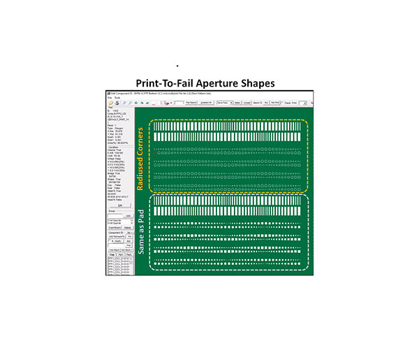
Figure 1. Print-to-fail patterns and aperture shapes.
The PTF patterns have pads that are square, circular or rectangular, solder-mask- and non-solder-mask-defined, in widths of 3 to 15 mils. Solder-mask-defined (SMD) pads are also referred to as simply “mask-defined”; non-solder-mask-defined (NSMD) pads are also referred to as metal-defined or copper-defined. Each pad’s corresponding apertures are either the same shape as the pad (S) or are square/rectangular with radiused corners (R). There are 32 datapoints on each print. Each dataset is made up of 20 prints, for a total of 640 datapoints for each combination of shape, definition, size and aperture geometry in the database.
Four stencils were tested: 2- and 3-mil thickness, with and without nanocoating.2,3
The solder paste used in this test was Indium 8.9 HF Type 5-MC. The powder particle size distribution was the standard 15-25µm diameter. Type 4 was tried but showed too much variation on thin foils to be considered acceptable; therefore, the results for the Type 5 solder paste are analyzed and presented.
Execution. Print tests were performed in Koh Young America’s demo room in Duluth, GA, using the following equipment set:
- Printer: MPM Momentum BTB
- Support tooling: Quick Tool; three modules
- Clamps: EdgeLoc with retracting top foils
- Squeegees: MPM FP100, 250mm length
- Stencils: 2- and 3-mil BlueRing Nano-Slic Gold and Uncoated Fine Grain (Slic) stencils
- SPI: Koh Young 10µm aSPIre3
- SPI height threshold: 20µm
The print parameters were:
- Speed: 30mm/sec
- Pressure: 7.0kg
- Separation speed: 5.0mm/sec
- Separation distance: 3.0mm
The understencil wipe parameters were:
- Speed: 30mm/sec
- Sequence: wet/vac/vac or wet/vac/vac/dry
- Frequency: 1 (after each print)
Each test run began with four to six knead strokes to ensure the solder paste reached its working viscosity and two to seven setup prints to verify proper print performance and paste alignment before running the 20 data-producing prints. Execution time for the tests were approximately 30 minutes each, with continuous printing, under wiping and inspection.
Analysis. Data were exported to a .csv file and imported to Excel for manipulation. A pivot table was created to review the solder paste volumes, TEs and CVs. Appendix A (online) has details on the data manipulation methods.
Process capability and the coefficient of variation. The coefficient of variation (CV, CoV or CofV) is calculated as the standard deviation of a population divided by its mean. Applied to solder paste deposits, CV represents the spread of the volume, height, area or offset data. Because the average volumes of solder paste deposits vary based on many input variables, basic standard deviations should not be used to evaluate different distributions of data. Expressing the variation as a percent of the average normalizes it for better comparison.
As solder paste deposits become smaller, minimizing their variation becomes more critical:
- As passive devices get smaller, they are more prone to positional, rotational or tombstone-type defects related to print quality.
- As integrated circuit packages get smaller and leadless, they are more prone to head-in-pillow, insufficient solder joints, voids and intermittent opens related to print quality.
Controlling the variation in print volumes limits the opportunities for defective solder joints and their associated rework or failure costs.
A widely accepted guideline for solder paste deposit CVs is:
- <10%: preferred
- 10-15%: acceptable
- >15%: unacceptable
These guidelines are based on statistical process control (SPC) principles. Assuming a normal distribution of data as seen in FIGURE 2, 99.7% of the data should fall within +/-3 standard deviations of the mean. If we apply a typical SPI control limit of +/-50%:
- CVs of 10% will produce 99.7% of deposits within +/-30% of the target volume, leaving plenty of room for outliers or special causes of variation.
- CVs of 15% will produce 99.7% of deposits within +/-45% of the target volume, leaving little room for variation.
- CVs of 16.7% or higher will produce deposits outside the control limits, indicating an out-of-control process.4
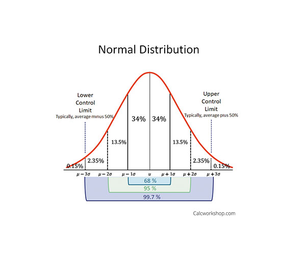
Figure 2. Normal distribution as it relates to solder paste volume variation.
In this study, CVs were analyzed first to distinguish datasets worth investigating from those that were not. Datasets with CVs of 15% were reviewed prior to inclusion into the database.
Disqualification of the smallest deposits. Upon review of the data and PCBs, 3- and 4-mil deposits were removed from the results. Their CVs were all greater than 15%, and inspection of the PCBs revealed many of the NSMD pads less than 5 mils were missing from the bare PCBs. This did not come as a surprise, as features that size present challenges to fabricators, which were granted waivers for features 5 mils or less.
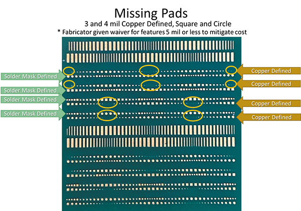
Figure 3. Missing pads in PTF test patterns.
The pivot table results of the different combinations of foil thickness, coating, pad shape and pad definition and the calculated CVs can be seen in Appendix B (online).
Unacceptable levels of variation were demonstrated by the 3- and 4-mil feature sizes; further statistical analysis was performed on the data from pads 5 mils and larger.
Results
The SPC run charts shown in TABLE 1 illustrate the effects of pad definition. There is a sharp contrast in print variation between the solder-mask-defined and copper-defined pads. In the best-case printing scenario of solder-mask-defined square pads, the CV of 12% indicates 5-mil features can be printed-repeatably using a 2-mil coated foil; the CV of 11% indicates the same for a capability with a coated 3-mil foil.
Table 1. Pad Definition Effects
The CVs for copper-defined pads were over 20% for both 5- and 6-mil features. The process of printing on copper-defined pads did not show preferred capability (CV<10%) until feature sizes of 7 mils, even with square pads, which performed better than round ones.
The transfer efficiencies also vary greatly between solder-mask- and copper-defined pads. Solder-mask-defined pads offer better gasketing than copper-defined ones, and limit the amount of “squeeze out,” or excess solder paste to transfer from the aperture to the PCB.
FIGURES 4 and 5 show the contrast in TE between the two pad designs for the 2- and 3-mil foils, respectively.
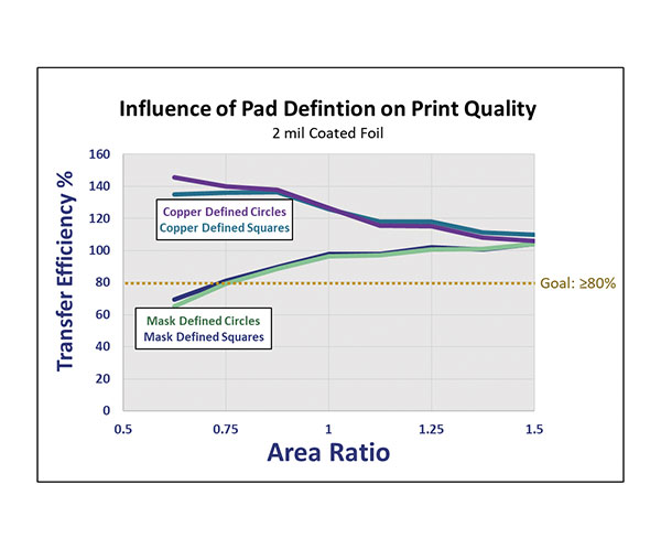
Figure 4. TE chart for 2-mil coated foil.
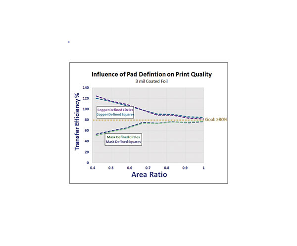
Figure 5. TE chart for 3-mil coated foil.
Regardless of foil thickness, the TE curves both show the same trends regardless of pad or aperture shape; for mask-defined pads, TEs showed typical behavior, but on copper-defined pads, excess paste was the rule rather than the exception.
On solder-mask-defined pads, TE is approximately:
- 70% at 5 mil
- 80% at 6 mil
- 90% at 7 mil
- 96% at 8 mil
These are all reasonable transfer rates with preferred or acceptable CVs.
On copper-defined pads, TEs averaged:
- 140% at 5 mil
- 140% at 6 mil
- 130% at 7 mil
- 125% at 8 mil
These TE rates, coupled with highly unacceptable CVs on copper-defined pads most likely indicate a lack of good gasketing between the pad and the stencil.
The run charts also show unanticipated spread in the data for prints 3, 13 and 19. The effects are more pronounced on the smaller features. This will be discussed in detail in the discussion section addressing pad definition.
The main effects plot shown in FIGURE 6 demonstrates the influence of the individual factors on print volume repeatability. The axis values have been omitted to focus on the relative impact of each and the inputs that minimize it.
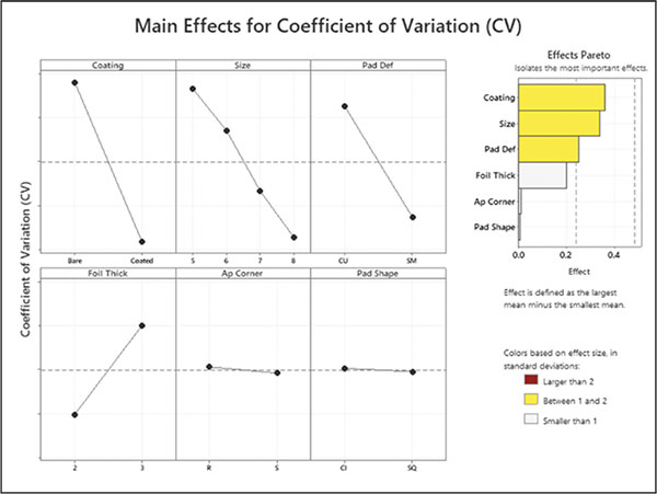
Figure 6. Main effects plot and Pareto diagrams.
The leading factor influencing print repeatability was the stencil coating. Feature size was a close second, followed by pad definition. With lesser influence, the 2-mil foil produced more consistent print volumes than the 3-mil foil. Pad shape and aperture corner type had negligible influence on print variation.
Discussion
Top factors in variability. As indicated in Figure 6, stencil coating is the top factor in minimizing variation. It is also obvious in the side-by-side comparisons of TE and CV in Appendix B, which show the coating provides better print repeatability (lower CV) for every pad design configuration.
Although not quantified, cleanability was a considerable factor noticed during the testing. It was observed that the coated stencil released the paste to the automatic underwiping system far better than the uncoated one. The thin layer of smeared solder paste particles and flux left behind on the stencil after auto wipe likely factored into its poorer print results.
The influence of pad size – the bigger the feature, the easier it is to print – is related to AR, but does not necessarily follow general AR rules.
Pad definition. FIGURE 7 shows a basic diagram comparing the two methods of designing PCB solder pads. Non-solder-mask-defined (NSMD) pads are etched onto the PCB at their nominal size. It is not uncommon, however, to find pads overetched – or undersized – by up to 2 mils.
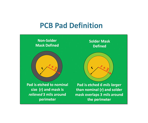
Figure 7. Comparison of PCB pad definition.
FIGURE 8 further describes features of the different types of pad definition. Given that smaller pad sizes are more susceptible to overetching, growing the copper size by 6 mils makes it much easier for the fabricator to etch; even it if gets overetched by (an acceptable) 2 mils, there is still room for the solder mask to encroach on all sides. When all edges of the pad are covered with solder mask, the mask provides an excellent gasketing surface for the stencil, resulting in less variation in print quality and, typically, slightly higher volumes.
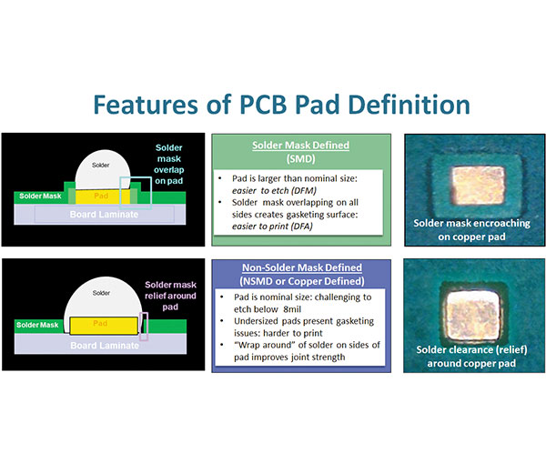
Figure 8. DFX impacts of pad definition.
When pads are metal-defined, they are naturally harder to gasket to than mask-defined pads, but their propensity to be overetched exacerbates the gasketing problem. Poor gasketing of NSMD pads leads to excess solder paste deposition, as seen in Figures 4 and 5.
Another deleterious effect of overetched PCB pads is their impact on true AR. Recall that AR is calculated as the ratio of the area of the aperture opening to its walls. This calculation is based on the assumption the aperture opening fully contacts the PCB pad. When the pad is smaller than the stencil aperture, it does not offer as much area for the solder paste to stick to, thereby reducing the true AR and introducing additional variation to the process.
Traditional pad design, especially for BGAs, generally trends toward NSMD pads, because the solder mask relief enables molten solder to wrap around the edges of the pad, giving the solidified joint more shear strength than with SMD pads (Figure 8). For larger BGAs with feature sizes that are more easily printed and experience greater displacement during thermal expansion, NSMD pads are still generally preferred, but in the case of very small features, mask defining them can add shear strength between the pad and PCB due to the larger area of the pad and the reinforcement of the mask.
As mentioned, the fabrication notes for this test PCB allow a waiver for pads 5 mils and smaller. Inspection of the incoming PCBs showed many were missing their 3- and 4-mil NSMD pads (Figure 3), and some of the 5-mil NSMD pads were barely visible. The run charts in Table 1 show excessive noise for print numbers 3, 13 and 19, particularly on the NSMD pads. The issue appears to resolve as the feature sizes get larger, and only appears on the smallest SMD pads. The source of the noise in these three prints could likely be attributed to overetch of the pads on those specific PCBs.
Aperture shape. Aperture shape had very little impact on print quality. This appears to contradict prior data generated on larger feature sizes and generally accepted design rules relating to radiusing aperture corners to improve paste release and repeatability.
Typically, stencil manufacturers put a 2-mil radius on square apertures, and often apply the “squircle” aperture to round pads. At feature sizes under 8 mil, the radius is 25% of the side length of the square. As the squares get smaller, and 50% of their side length is part of the corner radii, the squircle shapes become more circular than square, as seen in FIGURE 9, and the performance difference becomes relatively inconsequential.
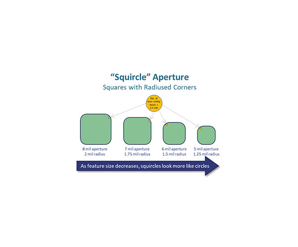
Figure 9. The effect of rounding aperture corners as aperture sizes shrink.
Pad shape. In a trend similar to the contradictory nature of the aperture shape results, pad shape had very little influence on print variability. The advantages of square pads (from a print perspective) also appear to dwindle as their size shrinks.
The area ratio rule. Area ratios increase as foil thicknesses decrease, but with foils less than 4-mils thick the difference is more dramatic (FIGURE 10).
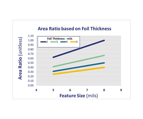
Figure 10. AR of small features increases dramatically as the foil gets thinner.
An 8-mil feature size has an AR of 0.50 on a 4-mil foil, 0.67 on a 3-mil foil, 1.0 on a 2-mil foil! Similarly, the AR for a 6-mil feature climbs from 0.5 on a 3-mil foil to 0.75 on a 2-mil foil!
With respect to print volume variation, size was a greater factor than AR. In many cases of mask-defined pads, variation was acceptable or preferred for features 5 mils and larger.
With respect to TE, pad definition had a far greater effect on print capability than AR.
In the best cases of SMD pads and coated stencils, 5- and 6-mil features were the smallest to print successfully – on both 2- and 3-mil foils. The lowest AR of this combo was 0.42, and the highest was 0.75. However, in other scenarios, acceptable printing wasn’t achieved until 8- or 9-mil feature sizes, with much higher ARs.
The area ratio rule of 0.60 or higher cannot be applied to all situations when using thinner foils. Considering foil thickness has four times the influence of aperture size on AR (the algebraically reduced AR calculation for circles is D/4t, where D is the diameter of the circle and t is the foil thickness and similar for squares as S/4t, where S is the side length of the square and t is the foil thickness), AR may no longer be the best overall indicator of solder paste release.
In this test, pad size and definition are the key design factors, and stencil coating is the key manufacturing factor. Size may be related to the three- and five-ball rules (yet to be discussed), but pad definition is related to design. Having the correct pad contact area to produce a true AR scenario and the benefit of good gasketing makes the biggest difference in printability of these fine features with thin foils.
When considering stepping a 4-mil stencil down to 2 or 3 mils to accommodate fine features, note in these tests, both the 2- and 3-mil coated foils printed relatively comparably. Given similar results between the two thicknesses and faced with a choice, an assembler might consider stepping down to 3 mils as opposed to 2 mils, as it would result in a more robust stencil with a longer production life.
Three-ball rule. The three-ball rule states a stencil’s thickness should be at least three times the diameter of the largest ball. A common corollary states it should be at least three times larger than the average ball diameter. It is illustrated in FIGURE 11.
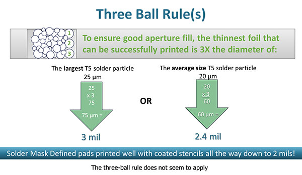
Figure 11. The three-ball rule.
The Type 5 solder paste had most of its particles in the 15-25µm range. Assuming the largest is 25µm and the median is 20µm, both scenarios can be theoretically tested:
- 3*25=75µm, or 3 mil
- 3*20=60µm, or 2.4 mil.
The thinnest foil to produce good prints was 2 mils. Again, it appears pad design and stencil coating enable this capability. For the uncoated stencils, the 2 mil printed better than the 3 mil for SMD pads; for the coated stencils, the 2- and 3-mil foils both printed comparably on the SMD pads.
The three-ball rule does not appear to apply to SMD pads in this test, perhaps because the mask definition creates a “well” that effectively increases the depth of the aperture with respect to solder paste filling, but does not negatively influence release from the aperture.
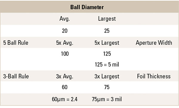
Five-ball rule. The five-ball rule states a stencil’s minimum aperture width should be at least five times the diameter of the largest ball. As with the three-ball rule, an existing corollary states it should be at least five times larger than the average ball diameter (FIGURE 12).
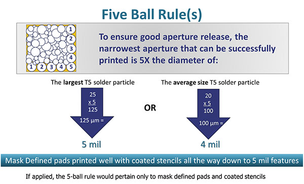
Figure 12. The five-ball rule.
So again, assuming the largest particle has a 25µm diameter and the median has a 20µm diameter, both scenarios can be theoretically tested:
- 5*25=125µm, or 5 mil
- 5*20=100µm, or 4 mil
The finest feature to print successfully on SMD pads was 5 mils. Even in the best-case scenario, the 4-mil pads demonstrated too much variation to be considered valid data worth analyzing.
To interpret the five-ball rule with respect to thin foil printing, these data indicate the largest ball diameter should be applied. It can only be applied to SMD pads, however, as NSMD pads produced unacceptable print volume variation.
Conclusions
In the context of solder paste stencil printing, reducing variation has always been as important as maintaining high transfer rates. However, in leading-edge electronic miniaturization, where excess variation is the root cause of most soldering problems, it is arguably more important than average paste transfer rates. This analysis reviewed transfer rates, actual volumes and variation, with the focus on factors that minimize variation.
Factors that minimize variation can be grouped into two distinct categories: design and manufacturing.
With respect to product design, solder-mask-defined pads and the sizes of those pads had the largest influence on repeatability. SMD pads are easier for PCB fabricators to make and easier for SMT assemblers to print. It is highly recommended any PCB features smaller than 8 mils should be mask-defined (when using a Type 5 solder paste), and as pad sizes get smaller, the positive effects of mask defining the pads become more obvious.
With respect to manufacturing, coating the foil with the flux-repelling ceramic nanocoating has the largest influence on reducing variation. In fact, on non-solder-mask-defined (NSMD) pads, uncoated stencils were not capable of meeting the preferred CV metric of <10% for any features 8 mils or smaller, and in only one situation met the acceptable value of <15%. Uncoated stencils were also very difficult to clean using automatic underwipe.
Foil thickness appeared to have a considerable effect on print variation; however, a very profound effect was seen on the uncoated stencils, and a detailed review of the actual results between 2- and 3-mil coated foils is extremely close with respect to both actual volumes and CVs.
With respect to traditional guidelines of the area ratio rule, the three-ball rule and the five-ball rule, some principles may still apply, and some may not.
In the context of SMD pads and coated stencils, an AR of 0.6 or higher can be applied to the 2- and 3-mil stencils. Both fell a little shy of 80% TE goals, but met CV goals of <10%, indicating viable processes that could likely be optimized with further statistical analysis of the stencil design and processing parameters.
The three-ball rule was tested with both the largest and average-sized solder particle and did not comply with the 3x guidance. It predicted minimum foil thicknesses of 3.0 and 2.4 mils, respectively, for the largest and average-size particles. The thinnest foil to print successfully was 2 mils thick, thinner than the rule predicts. It should be noted again the difference between SMD and NSMD pads was pronounced, and successful printing occurred on the SMD pads. SMD pads may offer an advantage in aperture filling due to the extra depth they provide, but do not offer a disadvantage in paste release, which is based on stencil wall contact.
The five-ball rule may still partially apply. The finest feature to print repeatably was 5 mils, or 125µm, exactly 5x the diameter of the largest ball, and only with coated stencils.
None of the 4-mil features printed repeatability, even when mask-defined and with a coated stencil.
DfX Takeaways
- The best thing designers can do to improve the producibility and reduce the cost of miniaturized electronics is to solder-mask-define the PCB pads.
- The best thing a PCB assembler can do to limit variation and improve yields is to nanocoat the foils, no matter how thin they are.
Potential Future Work
Similar tests using the same solder paste formulation5 have been performed with Type 4 solder paste and 4-mil foils. Those tests have indicated the T4/4 mil combination repeatably prints (CV<10%) NSMD pads down to 10 mil, and SMD down to 9 mil and, in some cases, 8 mil. Because the data were generated on different equipment sets at different locations and times, the data are not directly comparable. Ideally, however, a consistent data set that compares performance of T4 with 4-mil foil and T5 with the 4-mil foil can help determine the best print scenarios for features in the 6- to 10-mil size range.
Smaller particle sizes present greater reflow challenges. If possible, on future print tests, a few extra boards should be printed at the end of the test and reflowed to help determine fusion (non-graping) characteristics of the solder paste and the possible effects of inerting the reflow environment.
Ultimately, feature sizes will continue to shrink, and technology will continue to develop. Type 5.5 and 6 solder pastes will probably be tested in the near term, as will newer foil materials that can retain specific print properties with lower profiles.
Type 5 solder paste presented underside cleaning issues with uncoated stencils in this test. In other tests, it has also presented similar issues in offline stencil cleaning and misprinted board cleaning. Studies comparing the cleanability of wet T4 and T5 solder pastes would be beneficial to prepare for the inevitable transition to finer powders as electronic assemblies continue to shrink.
References
1. D. Dixon, et al, “Development of a Solder Paste Test Vehicle for Miniaturized Surface Mount Technology,” IPC Apex Expo Proceedings, 2018.
2. M. Bixenman, et al, “Quantifying the Improvements in the Solder Paste Printing Process from Stencil Nanocoatings and Engineered Under Wipe Solvents,” International Conference on Soldering and Reliability Proceedings, 2014.
3. N. Agarwal, “Evaluation of Stencil Technology for Miniaturization,” SMTA International Proceedings, 2016.
4. R. Welch, “SPI Data Analysis, Print Process Characterization/Optimization,” presentation, April 2019.
5. C. Shea, and R. Lawrence, “Solder Paste Qualification Testing for EMS Production,” SMTA International Proceedings, 2017.
is founder of Shea Engineering Services; chrys@sheaengineering.com. is manager of stencil technology at BlueRing Stencils; gsmith@blueringstencils.com. is customer program manager at Koh Young America; ray.welch@kohyoung.com.


