Processes for Building Test Boards
Migrating from manual to automated assembly and test.
Semiconductor companies pour millions of dollars into developing state-of-the-art chips like multi-core microprocessors, DSPs, FPGAs, ASICs, DRAMs and flash, among others. Semiconductor testing always has proven challenging. But as chips get more complex and smaller, the difficulties become even more apparent, both in cost and time. Successfully testing these advanced chips results in direct revenue for the company. Therefore, it often has high visibility from high-level management. That puts an enormous amount of pressure on test engineers to produce results, and they, in turn, rush their vendors, often pushing them up to and beyond their limits. As a result, extreme challenges are created for EMS firms involved in the assembly of ATE load boards.
A longtime industry practice exacerbates this issue. Previously, it was routine to manually assemble these boards, usually within a day or two, due to small order quantities. In the past few years, companies have been migrating to pick-and-place machines for better precision, accuracy and repeatability.
Although the assembly methods have evolved, standing expectations for turnaround time and pricing remain the same. Assemblers are pressured to quickly turn test boards and keep costs low, which proves difficult because of the tightly controlled processes involved. Manual assembly requires very little preparation, and its process is a lot more flexible in comparison. A typical pick-and-place/reflow assembly cycle is a few days due to a number of key considerations involved.
Test boards are bigger and thicker than regular PCBs. They are large, sometimes measuring up to 23˝ x 17˝, have anywhere from 22 to 42 layers, and are populated with thousands of components. They’re highly complex simply because they have to test innumerable chip functions, as well as simultaneously testing as many as 16 devices at a time.
A load board has a considerable amount of circuitry. That includes circuitry between components, as well as circuitry needed to connect to tester resources. Consequently, test boards tend to have considerably more gold and a high number of planes or metal innerlayers than conventional PCBs. Depending on the balance of these planes on a test board, and the board thickness, the board could draw a considerable amount of heat.
EMS providers are stepping in to move test boards to automated assembly. It’s not an easy path to forge. Test load board assembly has unique nuances and quirks that most assemblers may not properly translate.
That means having a good handle on correct thermal profiles, stencil cutting, pick and place, as well as understanding critical fabrication details.
Bill of Materials (BoM). Semiconductor test engineers traditionally generate the BoM from either CAD or schematic files. As a result, it’s not always in an ideal format to create the necessary programming at the assembler. In such cases, a general rule is flexibility, understand customer software capabilities, and work around them by taking the time to reformat the BoM. The trick is to do it accurately and still produce the intended result.
Like the BoM, auditing the parts kit for test board assembly is a bit different and should be handled gingerly, but expeditiously. Know what to question, when it’s important to ask, and when it’s not.
Semiconductor test engineers tend to expect the assembler to understand every nuance associated with their test boards, and these details will vary from one customer to another. That means they expect the assembler to know the parts to be used and any deviations needed. If every minor detail is questioned, it will delay the project. For example, if a BOM specs out a capacitor at a 5% tolerance, but the assembly house receives a better part with a lower one to two percent tolerance, they would normally consult the customer/OEM about using the lower tolerance part since it is a deviation from the BOM. The assembly process would be put on hold until the customer’s response was received. But that’s not so in the test world. It is extremely helpful for the assembler to learn which deviations are acceptable, specifically for a customer, and handle the issue quickly and accurately.
Thermal profile. Test board thicknesses can range as high as 0.187˝ to 0.250˝, with a high layer count that includes a number of ground and power planes, not to mention ample gold on the surface (typically 50 µ in of ENIG) on the tester and DUT pads.
The size of the board, along with the amount of metal it contains, places major challenges on developing a profile and arriving at the ideal temperature. Consequently, developing the correct thermal profile for a test board is very different than that for a commercial 0.062˝-thick, 12-, 14- or 16-layer board. Due to the sheer number of internal layers, considerable heat is required to bring the board up to a temperature for the solder paste to reflow. It’s important the heat profile is high enough for the paste to properly wet, while not so high that it damages the components or board.
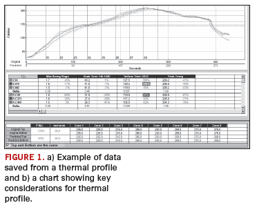
The challenge is to achieve the ideal temperature without burning the board or compromising the integrity of its various parts. Figure 1 shows an example of data saved from a thermal profile. It is normally archived with a job’s history in the event it needs to be referenced for future runs or to resolve issues. The chart shows key considerations when creating and defining a thermal profile.

Stencil. Cutting the proper stencil for solder paste application may seem minor, but the stencil plays a huge role in the success (or failure) of an assembly. For example, if an unusually small RF SMT component is involved, the stencil apertures must be accurately designed and cut to precisely accommodate it. Knowledge of stencil aperture patterns and their effect on solder reflow behavior is often overlooked. But if rework were necessary, it would defeat the purpose of moving the test board to automated assembly.
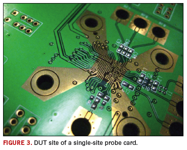
Also, if the stencil is not accurately cut, there can be dire consequences. For example, when running an improper stencil through pick-and-place and reflow, the result can be tombstoning and bridging (Figure 2). That can cause the board to undergo extensive amounts of touchup.
Placement. Some pick-and-place machines are not capable of handling test boards due to their rather large size. Therefore, it is important to audit the EMS provider’s equipment list for the proper placement machine.
Test load board customers are used to supplying small quantities of parts, usually in bulk or cut tape, and typically do not factor in part attrition. However, EMS companies require reels for pick-and-place, as well as an excess of components to account for part loss, usually expected with machine placement.
Moreover, setting up the machine requires files that weren’t necessary for manual assembly. Manual assembly can be performed with as little as a BoM (with its format not being an issue) and nothing more. Machine assembly requires a full set of files, usually Gerbers, IPC or centroid and X-Y data, and a BoM in a format that can be imported into the machine’s programming software. It is important for the EMS firm to convey these requirements to the customer before accepting and moving on with a project because customers may not be accustomed to providing, generating or acquiring these items if they have used only manual assembly.
Design for manufacturability is another issue the customer may not have needed to address with manual assembly. When a board is assembled manually, it is easier to work around DfM issues because a person can control and manipulate the part based on their observations. A machine will place a part based on the data it has been fed and cannot account for deviations, however subtle.
So to the customer, it may seem as if automated assembly introduces DfM issues, when in fact, those issues were already in existence, but not brought to his attention. The customer should be made aware that working around these DfM issues (as manual assembly would), may temporarily solve the problem, but is not ideal. The customer will benefit from DfM feedback because when addressed and resolved, the entire assembly process will be smoother and quicker.
Protecting the DUT. The device-under-test site (or sites) is the most important area of the load board. No matter how perfect the rest of the board is, if the DUT area is compromised in any way, the board can become useless. The EMS firm that is aware of this and pays attention to details can prove extremely valuable. For instance, nut fasteners (also known as PEM nuts) are often used to hold the DUT socket in place. To an average EMS, this may be a minor detail. An experienced EMS company will take great care to ensure the correct type nut is installed and that it is installed properly. Unlike other components on the board, a carelessly installed nut fastener sometimes cannot be repaired or reworked. If the PEM nuts on the board are not installed properly, the socket cannot be attached properly, which leads to not being able to load the DUT.
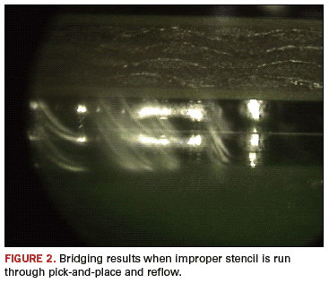
Protecting the DUT area while assembling a test board is a challenge (Figure 3). Most EMS firms use Kapton tape to protect areas on board during reflow. Kapton can sometimes leave a slight residue, which usually is not a problem with regular PCBs. However, DUT pads are more sensitive because Pogo or contact pins are used for board contact rather than conventional soldering. Because solderless pin contact is so critical, the DUT and test pads have to stay absolutely pristine during the entire assembly process – which EMS companies find challenging due to the number of process and people that the boards pass through. An experienced EMS company should be able to protect these vital areas from any type of contamination without hindering their normal assembly process. 
Board fabrication. Challenges are especially daunting for test board fabrication and certainly push the envelope. The high layer count of these boards means properly laminating 40 or more layers. The fabricator has to worry about tight impedance control, and because of the DUT package, these boards will often have blind and filled vias. ATE load boards also require stricter tolerances than what standard IPC guidelines dictate, and many fabricators cannot afford to accept and meet those tolerances. Although more fabricators are acquiring the experience, knowledge and equipment needed to build ATE boards, very few do it well.
Marilyn Ta is engineering program manager at Nexlogic Technologies (nexlogic.com); info@nexlogic.com.


