PoP Assembly Process Fundamentals
An elegant solution to space and weight constraints, PoP requires specific handling techniques and profiles.
Solutions for packaging multiple die elements in a single package outline have evolved rapidly. Vertically stacking several semiconductor die on a single semiconductor package substrate proved efficient for a number of high-density memory applications. When mixing some newer multiple function processor and controller products with more mature, high yielding memory die elements, however, the overall package yield did not always meet expectations. A solution that has proved more efficient is a package-on-package (PoP) methodology designed to vertically combine fully packaged and pre-tested discrete logic and memory on separate array configured package substrate levels that are designed to align and mount on top of one another (see cover).
Package stacking is proving ideal for a variety of applications requiring greater functionality, higher performance and a smaller footprint: Stacking pre-tested package sections enables a high degree of flexibility for designers, permitting virtually any combination of memory to be combined with any logic chipset. Combining discrete logic and memory packages in this vertical configuration not only saves space on the circuit board, it typically reduces pin-count, simplifies system integration and enables enhanced performance. A number of products are already taking advantage of this multiple die packaging solution, including wireless handsets, digital cameras, portable game players, and GPS products.
Cellular handset designers in particular are faced with providing more features in smaller and lighter form factors. Because many stacked PoP memory products are furnished with a consistent footprint and pinout, users can easily configure variations that meet different product applications or incorporate new flash, SDRAM or other devices as they are introduced.
When the PoP device is furnished to the user pre-joined, the package can be mounted onto the circuit using conventional SMT soldering processes. These products are furnished as fully tested single package units. Some users will insist the sections be furnished as separate pre-tested packages ready for joining during the board-level assembly process. The latter version enables flexibility in system configuration and supply chain management. In either case, these devices are normally compatible with existing surface mount assembly process methodologies.
Whether the IC package sections are manufactured within a closed (in-house) environment or supplied from outside sources, quality and integrity of the end product is paramount. However, source and configuration control and material tracking throughout the life of the product are also a concern. Each package section has been electrically tested before PCB mounting, assuring users that multiple die PoP products will meet all performance criteria. Even when IC package sections are furnished by different offsite suppliers, the logic device supplier is responsible for assembly and test for the logic section, and the memory manufacturers are responsible for assembly and testing of the respective memory section.
The base package and top package units are furnished with alloy spheres compatible with most lead-free solder compositions. If users choose to perform the joining of the package sections during board-level assembly, they will need to consider placement machine flexibility. Depositing solder paste on a circuit board is most commonly performed using a stencil printing process, providing solder to all component attachment sites with a single process step. Mounting the upper section will require a different strategy, however. Due to the physical profile of the base package unit, depositing solder paste on attachment sites distributed on the narrow top edge of the base unit is somewhat of a challenge. Stencil printing solder paste at these contact sites is really not practical. Component suppliers have successfully adopted several alternative methods to accommodate attachment of the upper package section. This includes solder paste and flux paste dispensing at each contact site, solder flux-dip transfer and solder paste-dip transfer to the upper package section before placement on top of the lower package section.
Dip transfer process. A number of solder suppliers offer dip transfer-compatible solder paste. Indium, for example, offers a halogen-free material (Indium8.9-HF) in two alloy configurations: SnPb eutectic and SAC 305. Solder paste is applied to the spheres using a dip-transfer process. The material is systematically maintained in a shallow reservoir at a precise level using a doctor-blade mechanism. To monitor this procedure, newer generations of pick-and-place systems are equipped with bottom-focused digital cameras that, when programmed, can detect missing solder ball contacts or contact without the correct volume of flux or paste coatings. Typical PoP applications only require 25 to 45% of the sphere height to be coated with flux or solder paste. When solder paste is involved, care must be taken to avoid contaminating the bottom of the package itself with the fine-grain solder paste, as this may cause bridging defects.
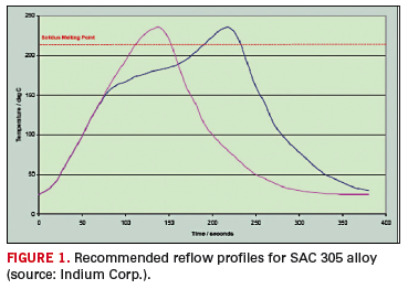
The peak reflow temperature will vary with the alloy type. Solder suppliers recommend a short preheat (140° to 150°C for SnPb37 and 150° to 160°C for SAC 305) for less than 45 sec. to reduce any solder balling caused by excess paste. Reflow solder profiles typical of those shown in Figure 1 should ideally be a linear ramp at 1 or 2°C per sec., up to 20° to 30°C above solidus temperature. The minimum time above liquidus should be 20 sec., followed by a rapid cool down to reach the solidus state.

A number of assembly systems available have been configured to accommodate 3-D package stacking and have included dip-tray stations between the package pickup location and the board. This feature was originally intended for flip-chip assembly processing, but works just as well for PoP applications (Figure 2). For optimum performance, the manufacturer recommends storing solder paste syringes and cartridges tip down at ≤10°C for maximum shelf life. Storage temperatures should not exceed 30°C for more than four days. The material should be permitted to stand for at least four hours at room temperature before using. Once removed from cold storage, the solder paste in a sealed syringe may remain at room temperature for up to seven days before and during usage. However, once outside the syringe, its working life is estimated to be no greater than eight hours, and may be less under high temperature (>25°C) and humidity (>70% RH) conditions. Further, the paste should not be subjected to multiple cold/heat cycles because viscosity can change and flux separation may occur. A number of materials have been formulated for no-clean applications, and can be left in place on the final package. However, when necessary, flux residues can be removed by using commercially available flux cleaner.

Post-assembly process evaluation. One of the challenges PoP device suppliers faced was managing the CTE mismatch and modulus variation of the dissimilar materials within a package. Although the PoP device will experience several levels of temperature exposures during assembly processes, the plastic-based components are expected to meet acceptable planarity and flatness requirements. The JEDEC 95-4.22 design guide document recognizes the relatively wide differences between the die element and resin-based materials used in the package assembly process. The standard, however, does not specifically define “flatness” criteria, but it does establish a parallelism tolerance of 200 µm for controlling the orientation of the top surface of the package with respect to the seating plane. The planarity limit of the seating plane contact features must be within 100 to 120 µm (depending on the ball diameter used). Even so, the tandem package configuration may be prone to some degree of package warp during the board-level assembly process, due in part to the physical variation between the resin-based multilayer circuit board material and the relatively thin resin-based package substrate materials. The primary concern is that if this warp condition is excessive, it can cause random solder defects that will compromise product reliability or prevent proper functionality.
Physical reinforcement. Many of the BGA-configured PoP products are targeted for the commercial wireless handset market. Because these handsets are subjected to various degrees of physical shock, vibration and thermal gradient extremes, some manufacturers of these products will physically stabilize the array packages with an epoxy resin underfill. The liquid underfill material is typically dispensed at the package edge and, by capillary action, flows under the device, furnishing a mechanical bond between package and PCB. Several different types of underfill are used. The most commonly used underfill compounds are referred to as snap cure, low profile, high performance, and reworkable.
To reduce voiding and ensure proper flow and adhesion of the underfill material, the surfaces of the PCB and package substrate must be free of flux residue. In addition, component suppliers warn that most materials used for both underfill or molding are sensitive to moisture absorption.
Substrate warping. Primary markets for the PoP devices are miniature portable products where package outline, profile height and package warp must be minimized. Substrate warping has plagued the multi-level package products throughout their relatively brief history. Manufacturers recognize the negative warp effect of the outer edge area of lower package interposer. During the package-to-board assembly process, if the base (or lower package) substrate flexes downward at its edge, the solder ball contacts mating with the host PCB can collapse to the point of merging together. Likewise, if the second-level package substrate warps in the opposite direction of the lower package, the solder interface will elongate and possibly separate.
Package assemblers have noted that most upper-level packages will have two or more die. The accumulated die thickness, along with the physical support of a high-temperature mold compound, considerably minimizes the warp condition. However, where the die element and mold compound on the lower package helps to minimize warping in its mid-section, the unsupported, relatively thin perimeter area is not restricted. This is the portion of the package that is configured to join with the upper level package and is more prone to warping.
Additionally, users expect future generations of PoP to furnish significantly greater functionality. Due to the increased complexity of the logic die elements and the demand for greater memory capacity, more contacts will be needed for both the upper and lower package sections. For many of these applications, OEMs would like to limit the outline to 12 x 12 mm (10 x 10 mm would be even better). The current JEDEC design guide standard defines a minimum contact pitch of 0.50 mm, allowing a maximum I/O for a 12 mm square configuration of 529, and only 361 I/O for a fully populated 10 mm square package. To meet the I/O density for the next generations of mixed function 3D packaging, many companies are anticipating the adoption of 0.4 mm and even 0.3 mm contact pitch.
Although widely used for single die wafer-level chip-scale package (WLCSP) and flip-chip applications, the finer pitch for an alloy ball or bump contact configurations on PoP applications are proving to be very difficult to manufacture. Some companies have found limited success by printing and reflowing solder onto the ultra-fine pitch contact sites, but profile uniformity of the contact features do not always meet the established criteria for planarity.
Avoiding the need for underfill is also a goal for many companies manufacturing products in high volume. Until this process stage, everything is running hands-free and smoothly through a series of conveyor transfer systems, from package placement to reflow and cleaning. The assembly is then transferred to a dispensing station for applying the underfill material and, for some materials, a curing cycle that could be as long as one hour. Add to that the detection and correction of any solder process defects or package removal and replacement may be difficult or not practical.
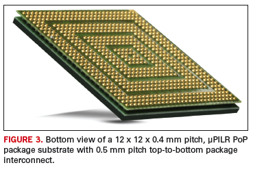
A viable solution has been developed to provide finer pitch and higher contact density for PoP applications. A unique substrate interposer fabrication process now available furnishes solid raised copper contact features for package stacking and board mounting in place of the ball contact features. This µPILR provides significantly smaller contact feature and finer pitch variations of 0.40 (Figure 3) down to 0.35 and 0.30 mm.

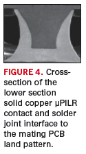
When comparing the µPILR contact profile to the more common solder ball connections, the contact geometry is significantly smaller in both diameter and height, enabling a much lower finished package profile. The solid copper core contact (Figure 4) is slightly tapered in shape and coated with a nickel/gold (ENIG) alloy that is compatible with either eutectic or lead-free soldering processes.

Assembly of the µPILR package-on-package device is very typical of most surface mount processes, beginning with solder paste printing, pick-and-place and reflow soldering. The stencil successfully used for printing is a 100 µm thick stainless steel foil with laser ablated 270 µm square apertures. Because of the very small stencil aperture, the recommended solder paste used for this application is a Type 5 powder size. Precise placement of the 0.40 mm pitch components is critical as well. When placing ultra-fine pitch array devices, machine placement accuracy should be in the range of +/- 20 µm to ensure a reasonably uniform solder fillet at all contact sites.
One of the benefits of the package substrate structure is the ability to reduce interconnect solder volume and tailor the solder shape to permit closer spacing of interconnects between package and board. An extended solder wetting plane provided by the package pins makes the µPILR less susceptible to solder defects caused by the warping typical of the BGA configured devices. Also, it does not require post-assembly underfill for mechanical stability or reinforcement. This is due to the solid copper pins providing crack stop reinforcement against solder fatigue cracks resulting from mechanical shock or thermal cycling. Reliability tests have shown the novel PoP to outperform the BGA PoP and exceed customer standards in drop testing and temperature cycling by 3 to 8 times without underfill.
Vern Solberg is founder of ST Madison; vsolberg123@aol.com. Phil Damberg is vice president, operations, interconnect, components & materials, at Tessera (tessera.com).


