PCB Design for Defect-Free Selective Soldering

General guidelines for SnPb and Pb-free alloys.
Increased PCB complexity and component density make selective soldering a popular technology, especially when the ratio between surface mount and through-hole components is high. As a replacement for hand soldering or wave soldering with pallets, selective soldering offers many lead-time and solder joint quality advantages. The selective soldering process has unique factors related to the machine design. To develop a robust process, PCB design plays a key role.
PCB or pallet dimensions. The maximum dimensions depend on machine type. The maximum is 610 x 610 mm, while the minimum is 100 x 150 mm. For smaller PCBs, pallets should be used.
PCB warpage. The tolerance for PCB warpage is less than 1% of the PCB diagonal dimension. In a single wave selective process, additional supporting or vacuum pins can be used to control warping. Machines that use multiple waves can handle slightly more warped PCBs due to compensation mechanisms on the plate.
PCB weight and distribution. The maximum PCB weight, including the PCB gripper and pallet, is 15 Kg (33 Lb). In addition, the maximum weight concentration for a particular area for a 100 mm2 or larger PCB must be limited to 1 kg.
Edge clearance. The edge clearance on top and bottom of PCB must be 3 mm. This clearance is necessary to support the PCB on the chain conveyor and the clamping fingers of the PCB gripper.
It is possible to use edge components, as long as there is enough free space to support the PCB. The distance between edge components and the PCB corner should be 28 mm to provide enough space for the clamping fingers of the PCB gripper and position pins. The number of clamping fingers should be sufficient to prevent board warping, and the distance between edge components where the clamping finger will be placed should be at least 26 mm (the width of clamping fingers).
Cutout areas of supporting edges may affect the PCB handling on the pin-chain of the conveyor system. It is recommended to provide breakout parts for such areas where breakout parts can be removed after assembly.
Positioning holes. Two position holes are preferred for precise board positioning. Preferably, one round hole and one slotted hole should be available on the fixed rail side of the PCB. The slotted hole reduces board bending when PCB expansion/contraction occurs during soldering. Hole diameter should be between 3 and 5 mm. Keep the holes outside the 3 mm edge clearance area and keep a free space of 8 mm diameter around these holes.
Lifting areas. At least four areas of 6 mm diameter on the board bottom along the length of the conveyor direction are required for lifting the PCB from the pin-chain conveyor. These supporting areas are normally within a zone of 10 mm, measured from the PCB edges. The total number of lifting support pins must be selected in order to provide a stable PCB during the lifting operation.
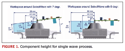
Component height. The general specification for component height on the top side of the PCB is 120 mm. Component height on the solder side is 25 mm for a multiple wave process and between 6 and 40 mm for single wave process. This large range depends on the component position in relation to the soldering area and soldering angle (Figure 1).

Clearance between components and board. There should be at least a 0.5 mm gap between the component body and the pad on the component side. This permits flux vapors to escape and reduces opens. One cause of open joints is flux vapors escaping via the solder side of the PCB.
Lead protrusion. Lead protrusion depends on the PCB type. For single-sided PCBs, the lead length should be at least half the pad size, while for double-sided PCBs where the PTHs are completely plated, the lead protrusion should be at least 25% of the pad size.
When a dip soldering process is used, lead protrusions up to 10 mm can be used. However, when a drag process is used, the lead protrusion can go up to 4 mm to avoid bridging.
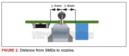
Surface mount devices proximity. Free space around selective soldering joints is necessary to have free access to the nozzle and to reduce thermal load to the surrounding components. In general, a free space of 4 mm should be used. This is measured from the center of the solder joint to the surrounding components/joints. The 4 mm is based on 3 mm (joint to inner nozzle wall) + 0.5 mm (nozzle wall) + 0.5 mm clearance (Figure 2).

When a drag soldering process is used in a single wave process, the free space depends on soldering angle and/or height of the components. In a single wave process, a minimum distance of 1 mm is possible, provided there is sufficient free space at the opposite side of the solder joint for placing the minimum admissible diameter nozzle (Figure 4). For a multiple wave soldering process, the distance can be 2.5 mm.


Gap between nozzles and PCB. When nozzle plates are provided with standoff pins, the pins will keep a gap between PCB and the top of the nozzle at a fixed distance. The distance can be between 0 and 1.5 mm. The most common gap is 0.3 mm.
These are general guidelines to consider when designing a PCB for a selective process. These recommendations will ensure minimum defect process when the optimal process parameters are used. For specific applications, contact Lammie Willemen (lwillemen@vsww.com) or Chris Curole
(ccurole@vsww.com).
Ursula Marquez de Tino, Ph.D. is a process and research engineer at Vitronics-Soltec, based in the Unovis SMT Lab (vitronics-soltec.com); umarquez@vsww.com. Her column appears monthly.


