Open Circuit Via Hole
Poor plating can be a culprit, and audits are in order.
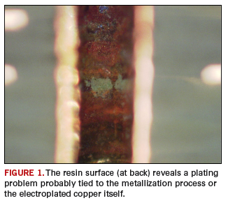
This sample via hole (Figure 1) has been mounted in resin and microsectioned to look at the plating quality. The optical image clearly shows the resin surface at the back of the hole. This is a through-hole plating problem, and closer examination of the plating is required. The center of the sidewall may show the problem relates to the initial metallization process or the electroplated copper. The poor coverage in this example could have been caused by residues on the surface of the drilled hole that were removed during plating. Or, it could be related to a gas bubble in the hole during plating. In the case of less obvious examples, a light is put behind the microsection to show up the degree of laminate coverage.

Auditing the printed board fabrication process with samples examined from drilling through the final copper plating process should be considered. Optical examination of hole coverage and microsections should illustrate satisfactory process control.
These are typical defects shown in the National Physical Laboratory’s interactive assembly and soldering defects database. The database (http://defectsdatabase.npl.co.uk), available to this magazine’s readers, allows engineers to search and view countless defects and solutions, or to submit defects online.
Dr. Davide Di Maio is with the National Physical Laboratory Industry and Innovation division (npl.co.uk); defectsdatabase@npl.co.uk. His column appears monthly.


