Optical Inspection of Black Pad
Many gold failures are incorrectly attributed to black pad issues.
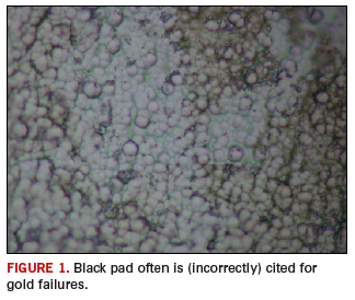
Figure 1 shows the surface of a nickel pad on a printed board after stripping the gold from the nickel surface. The image shows limited evidence of corrosion on the nickel surface at the grain boundaries on a bare board. Some evidence of gold is also still visible. Solder joint failures when examined normally show far more corrosion around the nickel boundary. Much debate centers around the subject of black pad. Changes to nickel chemistry and better control have reduced solder joint failures.

Unfortunately, many gold failures are attributed to black pad issues, when clearly they are not. Close cooperation is necessary with the PCB supplier and its chemistry supplier to determine the cause of the problem. Always ask to review the chemistry supplier’s audit reports conducted at the PCB supplier’s offices. Independent analysis also may be required, if the assembly processes are considered the root cause of any joint failure. Review the PCB fabrication process, the reflow temperature and time in a liquid state for the solder paste.
These are typical defects shown in the National Physical Laboratory’s interactive assembly and soldering defects database. The database (http://defectsdatabase.npl.co.uk), available to all this publication’s readers, allows engineers to search and view countless defects and solutions, or to submit defects online.
Dr. Davide Di Maio is with the National Physical Laboratory Industry and Innovation division (npl.co.uk); defectsdatabase@npl.co.uk. His column appears monthly.


