Second Source Need Not be Second Rate
Properly applied DfM mitigates component package tolerances.
You may have been here: John and Sally did the design and PCB layout for their company’s popular new product. It was, in fact, so popular, many of the primary-source components cannot be procured in the quantity necessary, so backup sources have begun to be used.
And that’s when the trouble began. Instead of the high yield they had been achieving, there were failures and, worse, intermittent problems began to surface. After a great deal of time investigating the cause, they discovered one of the components supplied by a secondary supplier was not quite mechanically equivalent. Unlike the initially sourced part, the solder points did not line up in the center of the lands.
This can happen with any product. However, very popular products that run for a long time are more likely to have to use second- or third-source parts over the run of the product. And, of course, a long-running, popular product is the last one in which you want to have quality problems arise.When a designer uses a land pattern for a single-sourced component, such as a programmable part, SoC, etc., the chance for subsequent manufacturing problems, due to the component not precisely matching the lands, is virtually zero. Lands were specifically designed for that, and only that, part. On the other hand, commodity-type parts are almost always multi-sourced, and not all suppliers have precisely the same component geometry.
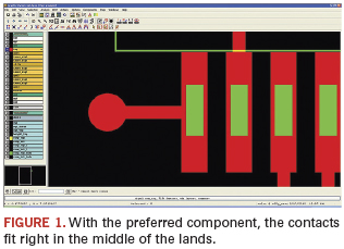
Here’s a real-world example: Figure 1 shows the contacts area of one possible component placement. Notice the size of the left and right distance present to supply enough solder on each side of the pin. In this example, the preferred component’s contacts fit neatly into the center of the lands generated from library data. Even if the component were slightly misplaced or dislodged, there is a cushion. Such margins enhance manufacturability and minimize rejects.

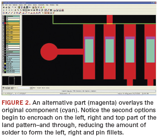
In Figure 2, a second-source component placement has been superimposed over the primary-source component. The cyan color represents the original component, and the magenta color represents the portions of the second-source component that extend beyond the bounds of the primary-source component. This part is now encroaching on the edges of the lands. Because the contact points take up greater area on the land, less solder is available to form an acceptable pin filet. While the component in this illustration may not produce manufacturability problems, in more extreme cases, contact points might take up too much area, or be near or off the edge, which can result in serious quality problems.

Rather than find out you have a problem when production yields take precipitous plunges, incorporate DfM practices early in the design process to ensure all possible components will be accommodated by the land patterns in the design library. (This, by the way, can be automated.)
On the horizon are tools capable of automatically generating an “envelope” that fits all available components. Then, the envelope is compared to the land patterns. Using the envelope approach ensures every possible component that can be sourced for this product will fit and pass a solderability test.
This problem is just one that can be addressed with DfM techniques and tools. In the future, I will illustrate other DfM techniques for PCB design.
Max Clark is product marketing manager, Valor Division, Mentor Graphics (mentor.com); max_clark@mentor.com.


