Successful ICT Boundary Scan Implementation

Eight steps to getting the best possible test coverage.
IEEE 1149.1 for boundary scan adoption has seen a steady climb in use for the past five years. In particular, it has gained popularity with NPI test engineers working with high node count printed circuit boards for telecom network servers/switches and PC servers. There are several ways to implement boundary scan test on PCBs, the two most common being:
- Native boundary scan on in-circuit test systems. (Note: Native boundary on ICT is an integrated solution where the boundary scan test will be developed and executed within the same ICT interface. No additional third-party hardware or software is needed.)
- Standalone benchtop boundary scan. Standalone benchtop boundary scan is preferred during prototype/NPI, as it enables PCB testing without building an ICT fixture. However, it has not been adopted for high-volume manufacturing, where the majority of manufacturers use the native boundary scan on ICT. Here’s why:
- Cost. A basic benchtop boundary scan setup is about $10,000 to $20,000. Additional licenses for development, debug and runtime features will increase the cost of the benchtop boundary scan solution up to two to three times the basic cost. Compared to the cost of using native boundary scan on ICT solution, the latter is practically free, as most EMS providers and ODMs would already have boundary scan licenses enabled on their existing ICT systems, which include development and debug features.
- Separate station. Running an extra station after ICT doesn’t appeal to most assemblers, as it means extra system and manpower costs, not to mention an additional process.
There are other minor reasons, such as local support, especially for the majority of high-volume manufacturing sites in Asia. Availability of expert support from the benchtop boundary scan vendors in Asia has not come far compared with that offered by ICT vendors. This is understandable, since ICT has been around for more than 30 years in electronics manufacturing, fostering a more robust support model.
These are just a few reasons why most assemblers prefer ICT for boundary scan test for volume products. Besides, ICT offers coverage for most of the PCB defect spectrum (opens, shorts), analog components value measurements, as well as powered test, which includes voltage measurements, clock measurements, digital test and in-system programming capabilities. Table 1 compares boundary scan test coverage of a typical benchtop boundary scan setup with an ICT offering boundary native scan capabilities. 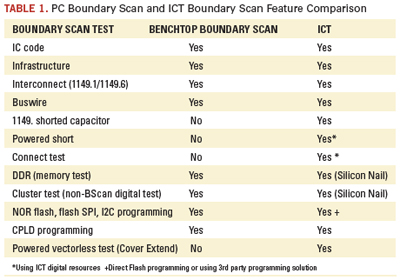
Although native boundary scan on ICT is the preferred solution during volume manufacturing testing, avoidable implementation issues can affect stability of the test.
Boundary scan tests, like any other digital test during ICT testing, are susceptible to noise, which affects stability. As such, the following best practices should be considered:
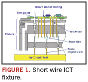
1. Assign critical attributes to JTAG pins (TDO, TDI, TMS, TCK and TRST) to ensure the shortest wire possible (Figure 1). To ensure signal quality and fidelity, consider assigning critical attributes to the JTAG pins during test development to ensure the fixture has the shortest wire possible (as short as 1") from the ICT system’s digital card pins to the test probe. The shorter the wire on those JTAG pins, the less the possibility of an adjacent wire crosstalk.
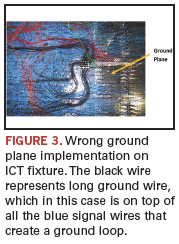
2. Proper fixture ground plane implementation. The main objective of using a ground plane on the ICT fixture is to reduce ground loop created by the distance between the ICT system ground and the PCB ground via fixture wiring. Unfortunately, few understand proper ground plane implementation, which can make or break the ICT digital or boundary scan test (Figure 2). The objective of having a proper ground plane is to help ensure the PCB ground is as short as possible to the ICT system’s digital ground during digital test, to minimize ground loop, as well as ensure that the signal wire stays closer to the ground to minimize crosstalk. Figure 3 is an example of a badly implemented ICT fixture ground plane, which is worse than not having a ground plane. 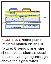
3. Twisted-pair wiring on JTAG pins (TDO, TDI, TMS, TCK and TRST). Aside from short wiring, another strategy to ensure signal integrity and minimizing noise is implementing twisted-pair wiring on JTAG pins. Twisted-pair impedance of approximately 100 Ω matches the low output impedance of the digital driver of the ICT system, which will result in a better drive signal integrity.
4. Removing physical test probes. For nodes that have only boundary scan devices connected to them (100% boundary scan nodes), removing these probes could ensure the signal integrity on those nodes stays clean. However, use a conservative approach in removing test probes on boundary scan nodes, as it will mean losing test coverage if there are non-boundary scan devices or analog components connected to it.
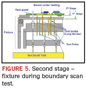
5. Dual-stage fixture. Most of the designs of high node count assemblies have resorted to a dual-stage fixturing solution where during the first stage, all the test probes are in contact while executing unpowered and powered in ICT (Figure 4). At the second stage, executed after all first stage tests have been passed, the fixture probe plate will move up either mechanically or via a pneumatic cylinder to disengage most of the normal test probes, with only a few long travel test probes remaining in contact. The test probes in contact during this second stage are power, ground, JTAG pins (TDI, TDO, TCK, TMS and TRST), as well as compliance and disabling pins (Figure 5). With the dual-stage fixture strategy, most noise coupled through the fixture wires is eliminated, resulting in a stable boundary scan test.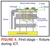
6. Power cycling or reset sequence. Adding a power cycling or reset sequence procedure to the test plan ensures the boundary scan devices in chains are in the proper state for testing. During boundary scan, the core logic of the devices in the chain is disconnected from the rest of the board, which probably would affect other devices operating in normal mode. Other devices exchanging data with boundary scan devices will consider the devices inoperable.
Note that when the board comes out of boundary scan mode, all the boundary scan devices go into BYPASS, and the core logic is reconnected to the I/O pins, but the board and the boundary scan devices do not necessarily pick up where they left off. To get the board back to normal operating mode, the board reset procedure must be run, or board power must be cycled. This can be done by adding a reset sequence or power cycling procedure to the test plan.
For multiple chains, interactions between chains can be a problem. For problems with connect tests or disabling difficulties, try adding a power cycling or reset sequence to the test.
7. Disabling upstream device, oscillator, switching voltage regulator. When a digital or boundary scan device is being tested, its surrounding devices can affect the way the device operates. This, in turn, can affect the test for that device, resulting in an unstable boundary scan test. To some extent, the effect that other devices have on the inputs to the device under test is minimized in the test system by overdriving. However, this is not always completely effective and cannot be used with high-speed signals. Disabling the upstream devices ensures that there is no other signal interference while executing boundary scan test. Disabling on-board oscillator and switching voltage regulators ensure that noise coupled through fixture wiring is minimized, which will result in a stable boundary scan test.
8. Maintaining JTAG pins signal during boundary scan test and disable state. Most PCBA with good boundary scan design for test implementation will take care of the pull-up/down resistor of the JTAG pins to ensure stability of the boundary scan test. If these DfT factors have not been included on the board, implementing them on the fixture will help.
The TCK (test clock) should be treated like any clock pin, although it has nothing to do with the on-board clock function. The TCK should be terminated with a 68 Ω resistor in series with a 100 pF capacitor to ground.
Maintaining stable TMS (test mode select) signals, either during boundary scan test or the disable state, is very important. During boundary scan test, the test generated by ICT will ensure that TMS will maintain its level according to the state diagram. However, during boundary scan test, disabled TMS should maintain a signal level to remain in the reset state. A pull-up resistor will help to ensure that TMS remains high.
TRST (test rest) is an optional JTAG pin designed to let the boundary scan test get into the TEST-LOGIC-RESET mode regardless of the state of TMS or TCK. Whenever TRST gets asserted alternatively in the absence of TRST pins, boundary scan will enter the TEST-LOGIC-RESET mode when TMS is held high for at least five rising edges of TCK. The TRST signal should include a pull-down resistor when possible to reduce the chance the signal floats when it is not being driven by the ICT driver.
The success of boundary scan test implementation on ICT lies not only with the tools used, but also the project team’s support of the strategy from design and test engineering up to production. With a new set of boundary scan-related IEEE standards (P1687, P1581, 1149.7, 1149.8.1) expected soon, boundary scan will get a further boost in the board testing environment.
Bibliography
1. IEEE, 1149.1-2001, “Standard Test Access Port and Boundary-Scan Architecture.” June 2001.
2. SMTA, SMTA/TMAG Testability Guidelines TP-101D, 2008.
3. Kenneth P. Parker, Boundary Scan Handbook, 3d edition, 2003.
Jun Balangue is technical marketing engineer at Agilent Technologies (agilent.com); jun_balangue@agilent.com.


