Mining Data to Improve Stencil Printing
An elegant method for sorting print data by component and defect type.
A mountain of data is a wonderful thing; it’s filled with gems of knowledge just waiting to be unearthed. While those precious gems are worth the hunt, prospecting for them can be a tedious task, fraught with dead ends in trial-and-error processes. Once a strong vein has been identified, however, it can be tapped over and again to provide good results.
Ray Whittier of Vicor (vicr.com) has developed a simple yet highly effective recipe for mining the data his solder paste inspection system acquires. On the production floor, the machine is essentially a go/no-go gauge, indicating which prints can be passed on to pick-and-place and which must be removed from production. To make that decision, the machine collects a lot of data for each individual deposit, including solder paste height, area, volume, and X-Y position, and associates each data point with the package type, reference designator, pin number, date, time of day, etc. While the machine is dutifully executing its primary function of passing or failing prints, in the background it is generating a mountain of data that, when mined astutely, provides excellent diagnostic information.
Whittier’s first step is to download the database to an Excel spreadsheet for easy manipulation. Then he starts slicing and dicing:
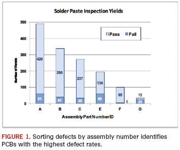
- The first cut is by assembly number. This identifies the assemblies with the highest defect rates (Figure 1).
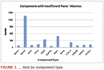
- The next cut looks at each of the top hitters individually. This view takes the data for each assembly number and carves them two ways:
a. By defect type (Figure 2).
b. By component type (Figure 3).
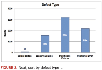
Sorting by defect and component type usually reveals a trend and points to the direction of the root cause. If a particular defect type is dominant, the root cause may be systemic. For example, if most failures are excessive solder volumes, he investigates the support tooling, looks for gasketing problems, and checks for undersized PWB pads. If the majority of failures are insufficients, he investigates paste release problems and checks for undersized stencil apertures that might drop area ratios (an aperture’s diameter divided by 4*foil thickness) below 0.66. If the defects are due to positional errors, he checks the printer’s program and the stencil positional accuracy.
Sorting by component type reveals the packages experiencing the most defects, and it’s no surprise the miniaturized components – 0.5 mm BGAs, 0201s and SOT883s – are the most problematic. To drill a little deeper into component-related defects, he looks at the defect modes and fallout rates of individual reference designators within the package types. Defects concentrated in a single location might be due to a tooling issue: a weak spot in the board support system, a component located near an edge clamp or irregularly formed stencil apertures. Drilling one step further to see the pin numbers where the defects are located identifies which apertures to check under the microscope. Alternatively, if defects are distributed across the board, he looks to the stencil, checking area ratios and measuring small apertures to make sure inadvertently undersized ones do not break the area ratio rule.
Download the data, filter it and sort it? It sounds almost too simple. Elegant is a better description, and successful. His process prints around 10,000 paste deposits in an area that’s roughly the size of a standard mail envelope at a 5.7∑ level. Impressive.
On highly miniaturized, densely packed PWBs, where one bad deposit causes an entire panel of 16 boards to get scrapped, the ability to quickly isolate and resolve the root causes of print problems is essential to an operation’s success. For Whittier, mining the data that his SPI system generates is one of the fastest ways to pinpoint the problem and get to its source. And while the method outlined here might not strike the mother lode every time, it always hits plenty of pay dirt.
Chrys Shea is founder of Shea Engineering Services (sheaengineering.com); chrys@sheaengineering.com.


