Via-in-Pad Myths

When it comes to heat transfer, bigger is not always better.
True or not true? When you need thermal vias, more is better; bigger is better.
Logically, this would seem to be the case. There are limits though, especially if you want a reliably assembled product. Older parts with heat slugs easily accessible for bolting on heatsinks didn’t have this issue. Just bolt on a piece of metal and maybe blow a fan across it. It’s different with a lot of the new, smaller surface mount packages. Many have a heat slug on the bottom, which requires carefully placed thermal vias to a copper pad on the underside of the board.
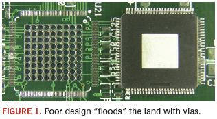
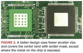
An extreme case of flooding the land with vias can be seen in Figure 1. In terms of assembly, you can hack this together for a prototype, but it’ll never fly in a production environment. It would be much better to use fewer smaller vias and have the center land covered with solder mask, except where the metal on the chip is exposed, as in Figure 2.
On the subject of vias, I’m sure you have seen charts on the current carrying capacity of traces, but what about vias? That’s a good question. I’ve heard that you first need to know the thickness of the via wall. Then, once you know that, the trace-width equivalent for the via can be calculated by using the formula for the circumference (diameter x ∏). For whatever number that gives you, compare the closest smaller trace width.
Now here’s a question for all you PCB fabrication gurus out there: Since vias are not created in the same way as the trace plating is, can that simple formula be used? While the trace copper is laminated onto a nice smooth PCB surface, the vias are typically created by deposition of copper dust in the via and then electroplating more copper. Then the surface finish is applied to all of the exposed metal. The via walls would generally be rougher than the flat substrate surface. Does that have an impact on the current capacity of a via?
Further, since airflow will be somewhat restricted in a via relative to a surface, should the via’s effective width be compared to an internal trace instead of an exposed surface trace? Should it be a compromise between the two?
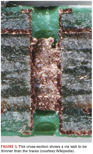
Look closely at Figure 3. The via wall looks thinner than the traces. You’ll have to make sure your board fabricator can give an accurate thickness of the via wall.
Ed.: Read Duane’s blog each week at circuitsassembly.com/blog/.
Duane Benson is marketing manager at Screaming Circuits (screamingcircuits.com); dbenson@screamingcircuits.com. His column appears bimonthly.


