Dendrite Growth Dynamics
Are industry standards sufficient for characterizing the effects of cleanliness at high voltages?
The increasing popularity of high-voltage electronics, particularly in electric vehicles, underscores the need to address the quality assurance and reliability challenges linked to these technologies. Standards, such as those published by IPC, are a great way to accomplish this. A crucial step to ensure the proper application of standards is to tailor them accordingly. For high-voltage electronics, an initial part of this process involves defining high voltage. Different organizations have already put forth their definitions.
For instance, the International Electrotechnical Commission (IEC) and British standards stipulate that anything above 1kV AC or 1.5kV DC constitutes high voltage. On the other hand, the American National Standards Institute (ANSI) categorizes high voltage as ranging from 115-230kV, extra-high voltage as 345-765kV, and ultra-high voltage as exceeding 1,100kV. When referring to IPC standards, however, which are more pertinent to the electronics domain, a provision in IPC-J-STD-001H states that the definition of high voltage hinges on the specific application.
For the scope of the arguments presented here, as the focus is on SIR testing and most SIR is conducted at 5V, it is reasonable to define anything above 5V as “high.”
High-voltage electronics are not new. Humans have been engineering products with high voltages for many decades including power transmission, scientific equipment like plasma treatment or MRI equipment, and even older CRT TVs found in many households a few decades ago. But if this is the case, why are high-voltage electronics still at the center of discussions at many industry meetings?
Considering the examples, they all have a few things in common. First, except for power transmission equipment, most high-voltage equipment lived in temperature- and humidity-controlled environments; if they didn’t, the cost of failure was relatively minimal. Second, although the instrument price might have been high, there was very little to no risk to human life.
To restate the answer, it’s all about reliability. With the advent of software-defined vehicles, which are essentially cars built around electronics, we are quite literally putting high voltage into the hands of the consumer. I am not necessarily referring to the charging adapters, but all the electronics inside of the car, which, if they fail, could cause serious injury or death. Imagine a dendrite being the cause of a car crash.
Given that high-voltage electronics have been produced for so long, one would think that there would be a well-established set of standards for manufacturing these high-reliability electronics. There is no argument that some electronic assemblies are deployed in harsh environments. Pick your favorite summer beach destination and imagine the stress those electric vehicle charging stations undergo. Huge temperature swings between direct sunlight and a cool, breezy night, rain every afternoon, salt spray from the ocean, and insect infestations that love to nest inside. Unfortunately, these are the environments to which these electronics are deployed, yet they are not being built to the standards required to ensure reliability. Things like good manufacturing processes (cleaning and coating) and, most importantly, testing of the assemblies, are key to reliability.
Is Elevated Voltage Testing Needed?
This work focuses on testing, specifically for dendrites in high-voltage applications. IPC has established performance classes to reflect the functional performance requirements, testing rigor and frequency. Class 1 electronics are those general electronic products where cosmetics are unimportant and failure is not impactful: devices like toasters or a light-up chew toy for a pet. Class 2 electronics are those dedicated service electronic products where high performance is required, and while uninterrupted service is desired, it is not critical. This classification includes equipment like an MRI machine. Class 3 electronics are those destined for high-reliability or harsh operating environments where continued performance is critical, downtime cannot be tolerated, and failure could mean the loss of human life. Among other requirements for Class 3, thorough cleaning and testing are essential.
The concern arises as to whether electronics operating at high voltages should be subject to testing at those elevated voltages or whether the conventional 5V test is deemed adequate. To navigate this question effectively, it may be helpful to review the current industry standards. IPC-J-STD-001, Section 8 on cleaning and residue requirements mandates the provision of objective evidence to demonstrate that a cleaning process results in an acceptable level of flux and other residues. This can include historical evidence, while surface insulation resistance (SIR) testing is recognized as a suitable measure to establish cleanliness for those lacking historical data.
To understand how SIR can be useful in providing the objective evidence needed to qualify a cleaning process, it is first necessary to understand that SIR is a measurement of the electrical resistance across two conductors on the surface of a circuit board. The idea is that the higher this resistance, the lower the level of contamination and the higher the reliability. In Figure 1, we see an example of a SIR coupon, which contains a BGA, a QFP, some QFNs, and a bank of capacitors; however, these can be designed to contain any number of various components to be representative of a specific assembly.
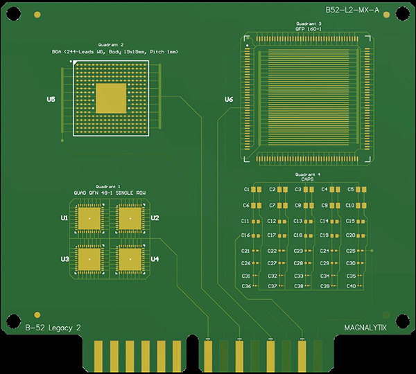
Figure 1. The SIR coupon was assembled with aBGA, QFP, QFNs and capacitors.
An SIR measurement is taken by first letting the representative coupon equilibrate in an environmental chamber. Typical conditions are 40°C and 90% relative humidity (RH), although other conditions can be used. A bias voltage of 5V DC is applied across the pattern, and the resulting current is measured. This current is then converted into a resistance using Ohm’s law. Measurements are then taken over the course of seven days. If, at any point during that time, the resistance value drops below a certain threshold value, then the test is considered a failure.
One aspect of this measurement that is commonly overlooked is the part about using Ohm’s law to calculate the resistance. Ohm’s law states that the current in a conductor is directly proportional to the applied voltage, which most people know as V=IR. However, the argument can be made that this is not the correct model for an SIR coupon. On an SIR coupon in an environmental chamber, many mechanisms contribute to current flow between the conductors, including electrolysis and reduction/oxidation reactions that may or may not be linear in nature (i.e., obey Ohm’s law). As seen in Figure 2, this is not a simple conductor.
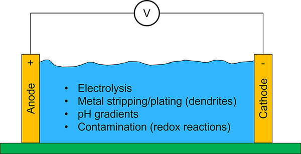
Figure 2. A visualization of some of the many mechanisms that contribute to current flow between the conductors.
Given these arguments, the question remains whether the current standards and test methods are applicable to these samples. Specifically, the time, temperature, RH, and pass/fail criteria. High voltages can affect materials by aging them, or if the voltage is high enough, it can experience dielectric breakdown. Also, the dynamics of dendrite growth at these higher voltages are under question. Do they grow faster or slower, and what role does contamination play in this?
Current IPC testing standards – IPC-J-STD-004C, 3.3.1.4 – state the SIR requirements for fluxes shall be determined in accordance with IPC-TM-650, Test Method 2.6.3.7, except that the test duration shall be 168 hr. The requirements for passing the SIR test are that all SIR measurements on all test patterns shall exceed the 100MΩ requirements after 24 hr. of exposure. That is the extent of the guidance given, unfortunately. There is no discussion about how higher voltages may affect the measurement.
SIR Test Protocol
Among the issues, dendrite growth dynamics is in question. A series of tests were carried out to understand how higher voltages affect dendrite growth. SIR test coupons were used to measure dendrite growth speed. One set of coupons was left clean, while another was contaminated with a commercial off-the-shelf no-clean wave solder flux. A droplet of DI water was placed on the surface to bridge two conductors. Various test voltages were applied up to 50V DC, and the time for a dendrite to grow across the 20-mil gap was measured.
Although applying bulk water droplets across the SIR pattern may not represent the adsorbed water layers on the surface during an SIR test, it can be argued that the mechanisms for ion diffusion through the water layer are similar. The tortuosity of the diffusion path in a thin layer will significantly affect the speed, and the results from this work will be orders of magnitude faster than would occur on a humidified board. The relative speeds of dendrite growth are of interest here to illustrate the effects of voltage and contamination, however.
Test Results
Figure 3 shows dendrites growing on clean substrates after 150 sec. at the stated voltages. Compared to dendrites grown on the contaminated boards after only 60 sec., a significant difference is seen (Figure 4).
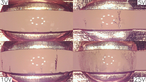
Figure 3. Dendrites growing on clean substrates after 150 sec. at the stated voltages.
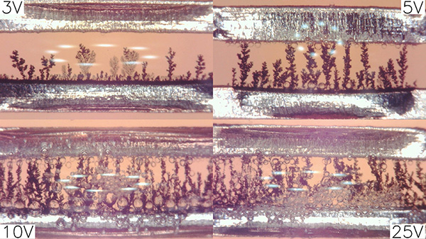
Figure 4. Dendrites growing on the contaminated boards after only 60 sec.
Qualitatively, the dendrites grow faster at higher voltages, regardless of contamination. However, they do grow significantly faster if the surface is contaminated. Another important observation is that more dendrites formed on the board in the contaminated samples. In the clean samples, only around five to 10 dendrites formed, whereas significantly more formed in the contaminated samples. Also interesting to note is that different dendrite morphologies exist. For example, the dendrites that formed at 25V on the clean sample are more ornate and coral-like, whereas the dendrites grown at the lower voltages look more like tree roots with only a few branches. At this point, the root cause of this difference is unknown.
Time measurements at each applied voltage were plotted and can be seen in Figure 5. The first thing to note is that the data was repeatable over the entire voltage range of 3-50V illustrated by the relatively small error bars. At 50V, the time to failure was less than one second and not measurable with the experimental setup. For this reason, voltages above 50V were not examined.
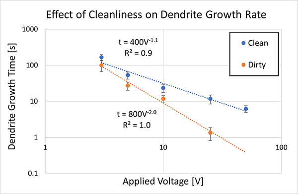
Figure 5. A plot of dendrite growth time and voltages on clean and contaminated boards.
What was observed in the videos can be seen quantitatively in the data. That is, higher voltages produced dendrites faster, regardless of cleanliness. This can be seen by the downward slope of the best-fit line (i.e., higher voltages took less time to grow a dendrite). Also, the dirty samples were faster across the board than the corresponding clean samples. The data also fit well to a power law relationship; the dendrite growth time of the clean samples was seen to be proportional to the inverse of the applied voltage while that of the contaminated samples was seen to be proportional to the inverse of the applied voltage squared. This suggests, not surprisingly, that other mechanisms are contributing to dendrite growth.
To visualize some of these mechanisms, a pH indicator was added to the water droplet, and the experiment was repeated. In Figure 6, a water droplet with phenolphthalein spanning three conductors can be seen approximately one minute after applying a 15V DC bias. PH gradients can be seen forming, as evidenced by the pink areas. Convection currents establish themselves within the droplet, and the pH gradient does not travel uniformly across the gap but ends up traveling in distinct lines. This further illustrates that the conditions on the surface of the board are not simple and homogeneous.
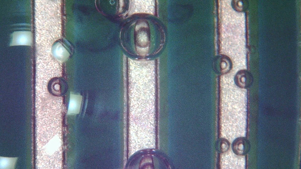
Figure 6. A water droplet and pH gradients can be seen on the board, demonstrating other mechanisms contributing to the dendrite growth.
Based on the results of this work, we can conclude that dendrites grow faster at higher voltages, and contamination exacerbates that growth. We also see that the dendrites are much more prevalent when contaminated. This is somewhat relieving as it suggests that the current SIR testing parameters, namely time under test, will bound potential failures. In other words, what would have failed during a standard 5V test will fail sooner at higher voltages and can be detected using current methods.
Conclusion
In conclusion, the chemical mechanisms occurring on an SIR coupon that contribute to the measurement are not linear, and blindly applying current standards when testing at higher voltages may be detrimental. Understanding these mechanisms with various contaminants will be key to determining applicable test parameters; however, it is important to note that although they might not be applicable, the current parameters do appear to bound the failures. For improved testing at shorter times, voltage-dependent testing will be required.
is director of science at Kyzen (kyzen.com); adam_klett@kyzen.com.


