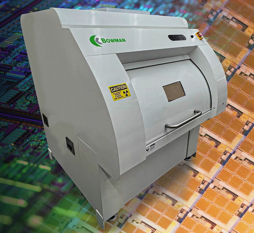
Bowman Introduces A Series Micro XRF
Bowman A Series Micro XRF measures smallest features on semiconductors and microelectronics.
Accommodates large PCB panels and wafers of any size for full sample coverage and multi-point programmable automation. Poly-capillary optics focus x-ray beam to 7.5µm FWHM. 140x magnification camera measures features on that scale; secondary low-magnification camera provides live-viewing of samples and bird’s-eye macro-view imaging. Dual-camera system lets operators see entire part, click image to zoom, and identify feature of interest. Programmable X-Y stage with movement of 23.6" (600mm) in each direction can handle large samples; precision down to +/-1µm for each axis; used to select and measure multiple points. Pattern recognition software and auto-focus features also do this automatically. 3-D mapping capability can be used to view topography of ENIG, ENEPIG, EPIG and other processes. Has molybdenum anode tube (chromium and tungsten also available) and high-res, large-window silicon drift detector that processes more than two million counts per sec.

Bowman
bowmanxrf.com


