SMTA Silicon Valley Chapter Membership Drive and Technical Presentation Meeting to be Held at Intel
SAN JOSE -- The SMTA Silicon Valley chapter will hold its first technical meeting of the year on Apr. 18 at Intel in Santa Clara.
The topic for this meeting is New Challenges and Opportunities in Packaging, Manufacturing Process for High-Density Multi-Chips. Sign-in and registration is 2:15 to 3:00pm, and presentations will be from 3 to 6pm. A reception will follow.
The meeting takes place at Intel SC12, 3600 Juliette Lane, Santa Clara. (Light refreshments to be served during breaks and registration.)
SMTA members and any guests may attend for free. Nonmembers: $20 (payable by cash or by check to SMTA Silicon Valley Chapter at the door.)
Schedule for the event:
2:15 - 3:00pm: Membership Presentation/Drive/Sign in table
3:00 - 3:30pm: Robert Blum – Director of Strategic Marketing and Business Development – Intel Silicon Photonics / The Datacenter – Integrated Photonics Manufacturing and Technology
3:30 - 3:40pm: Q&A
3:40 – 4:10 pm: Ken Brown – Senior Director, Packaging at Intel / Packaging - More Choices, More Complexity
4:10 – 4:20: Q&A
4:20 - 4:35pm: Bio/Coffee Break
4:35 - 5:05pm: Herb Reiter - eda 2 asic Consulting, Inc / Changing Market Requirements Bring New Challenges and Opportunities in Packaging
5:05 - 5:15pm: Q&A
5:15 - 5:45pm: James Rathburn - HSIO Technologies, LLC / Manufacturing Process for very high density multi-chip modules and circuits utilizing high performance Liquid Crystal Polymer (LCP) material sets in multi-layer constructions.
5:45 - 5:55pm: Q&A
5:55 – 6:00pm: Wrap Up
6:00 – 7:00pm: Social Hour
Speakers
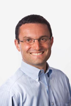
Robert Blum, Intel Corporation

Topic of Presentation “The Datacenter: Integrated Photonics Manufacturing and Technology”
Robert Blum is Director of Strategic Marketing and Business Development for Intel’s Silicon Photonics Product Division. Prior to joining Intel, Robert was Director of Strategic Marketing at Oclaro Inc., and held various Director of Product Management and Marketing roles for Oclaro’s telecommunications products and consumer laser portfolio. Before joining Oclaro, Robert was Product Line Manager for optical transmission components at JDS Uniphase Corporation and held various engineering and marketing management roles at Gemfire Corporation, all in California. Robert worked at Deutsche Telekom’s research labs in Darmstadt, Germany, while completing his master’s thesis and holds a doctorate degree in Physics from the University of Technology in Hamburg. He has also studied and done research at Ecole Polytechnique Fédérale in Lausanne, Switzerland, and at Stanford University, California.
Abstract: The rapid growth in data center traffic is driving the need for increased performance and overall bandwidth of networking equipment, including optical interfaces and Ethernet switches, which are based on pluggable transceivers today. But looking just a few years ahead, bandwidth scalability challenges are looming in terms of density, cost, and power; challenges that require tighter integration of optics and networking silicon. We will review motivation for integration and the enabling technology elements, and discuss how co-packaged Silicon Photonics enables higher density, reduced power per bit, and ultimately the continued scalability of network bandwidth and performance.
Ken M. Brown, Intel Corporation
 Topic of Presentation: “Packaging - More Choices, More Complexity
Ken Brown is the Senior Director for Packaging at Intel’s Silicon Photonics Product Division, and splits his time between Santa Clara, California, and Chandler, Arizona. Ken joined Intel in 1998 following Intel’s acquisition of the Digital Equipment Corp. (DEC) semiconductor business in Massachusetts. At Intel, Ken has held a variety of positions, with 20 years in Intel’s Assembly and Test Technology Development (ATTD) group - as Director of ATTD-Asia responsible for packaging development of Intel’s Communication and Wireless products in China, Malaysia, and the Philippines; as ATTD Senior Director of Package Design; and prior to his current role, as Senior Director of Packaging for Intel’s Custom Foundry business. Before joining Intel, he had worked in a variety of positions over 17 years at DEC in assembly, boards, advanced development, and semiconductor packaging, He has been in the electronic packaging field for more than 30 years. Ken holds degrees in Mechanical Engineering and an MBA from the University of Massachusetts at Amherst and Northeastern University. He also holds several packaging patents, chaired the Semiconductor Research Corporation Packaging Committee, and has authored packaging chapters for University texts. Outside of Intel, Ken is an award winning photographer, and was fortunate enough to receive an Intel “Sustainability in Action” grant to create the world’s largest full-color, high resolution, underwater photograph of the Bloody Bay Wall reef in the Cayman Islands to highlight the reef’s changing biodiversity.
Abstract: Back in the “old” days of packaging, the REALLY old days, you just had a few choices. You went with a standard leadframe package or tooled up a custom leadframe if your volumes were high enough, dropped your chip on it, did the wirebonding and molding, and voila ! you had your packaged chip. Or alternatively, you got a hunk of ceramic, printed a circuit on it with thick film metal and dielectric, attached and wirebonded your chips, and once again you had your product. Not to turn this into a packaging history lesson, but then we started surface mounted packaging, at least doubling the choices with thru-hole packages and surface mount. Next came along limited and then broad application of flip chip packaging, migration from ceramic to organic flip chip packaging, and the growth continued. The growth of packaging has really followed the growth and diversity of the product needs for the chips. There is no end in sight, which I guess for the packaging engineer is a good thing ! This presentation will discuss the growth, diversity, and increasing complexity of packaging.
Herb Reiter, eda 2 asic Consulting
 Topic of Presentation: Changing Market Requirements Bring New Challenges and Opportunities in Packaging
After 10 years as board-level and system designer, Herb worked for about two decades for ASIC and EDA companies in both Europe and California. In 2002 he founded his own company " eda 2 asic Consulting, Inc." to focus on reducing the gap between the IC design and manufacturing camps. Since 2008, when he started the GSA's 3D-IC Working Group, Herb consulted on 2.5/3D-IC design and manufacturing topics with SEMATECH, Si2 and EDAC/ESD Alliance to contribute to the industry's transition from single-die SoCs to multi-die solutions in advanced packages. Herb frequently blogs about multi-die IC-related topics at 3D InCites, see http://www.3dincites.com/3d-context/ . He earned an MSEE and MBA in Austria, an MBA at San Jose State University and attended 40+ Continuing Education Courses at Stanford University.
Abstract: The increasing demand for higher performance per Watt, integration of heterogeneous functions, smaller form-factors, lower unit and development cost as well as shorter times to profit are just a few of the reasons why the semiconductor industry is making significant changes to traditional strategies and practices. The most visible and impactful of these changes is our focus on advanced packaging technologies. They are shifting a major part of the value creation from single-die SoCs to multi-die (sub) system solutions in a package. Unlike multi-chip modules (MCMs) in the past, today's multi-die packages are becoming more and more cost-effective and, thanks to the emerging die-package-board design flows, much easier to develop, manufacture and deploy. This presentation outlines major market changes, explains the resulting challenges for our industry and shows how innovative companies turn these challenges into opportunities for growing revenues and profits.
James Rathburn - HSIO Technologies, LLC
Topic of Presentation: Manufacturing Process for very high density multi-chip modules and circuits utilizing high performance Liquid Crystal Polymer (LCP) material sets in multi-layer constructions.
 James is the founder and President of HSIO Technologies, located in Maple Grove MN near Minneapolis. He was previously the founder of Gryphics, Inc. which was sold to Cascade Microtech in 2007. James is the author of over 80 patents related to high speed electrical interconnect and circuit fabrication and is responsible for advanced technology development at HSIO. James has over 30 years of semiconductor industry experience, and attended Marquette University's College of Engineering.
Abstract: HSIO Technologies has developed a new method for production of very high density multi-chip modules and circuits utilizing high performance Liquid Crystal Polymer (LCP) material sets in multi-layer constructions not possible with historical fabrication methods. The intended paper will describe the basic process sequences compared to conventional circuit fabrication methods, and identify unique design rules to enable much higher density and performance than previous use of LCP and like dielectric materials. Heterogeneous Integration examples aligned with the DARPA CHIPS program will be described and demonstrated with high layer count LCP SiP substrates with sophisticated Micro-Electronics Assembly techniques extending from surface mount through embedded active semiconductors with passive device integration. A manufacturing relationship with Benchmark Electronics and Lark RF Technologies focused on a RF and High Speed Design Center of Innovation will be described to illustrate the manufacturing process highlighting Test at Assembly technology highlighting the importance of Known Good Die (KGD) for any multi-die assembly especially when devices are embedded within internal layers of a high layer count substrate. The paper will use true to industry relevant examples of high density modules developed to validate process, performance and reliability requirements for high reliability applications in the Mil/Aero/Defense/Sat/Auto and Tele/Comm/Mobile/Computing industries. Signal Integrity analysis normalized from empirical measurement data from DC to 112 gbs and 110 GHz RF will be explained to highlight the benefits of LCP vs conventional material sets.


