Solder Pad Coverage with NiAu and OSP Finishes

Tricks to eliminate exposed copper.
This month we look at solder pad coverage. Some quality engineers still want to see solder coverage, regardless of the PCB surface finish. If they see the original surface coating, they become concerned, regardless of what is stated in IPC standards.
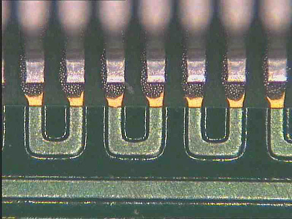
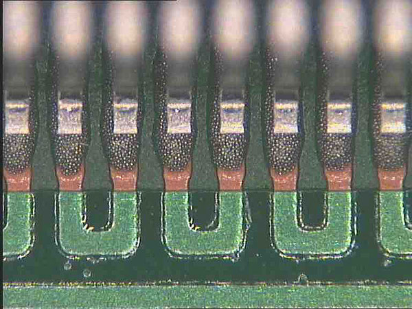
In the case of NiAu (FIGURE 1), it is most likely the solder paste will reflow and wet the pad toe area right up to the solder mask. In the case of an organic surface protectant (FIGURE 2), the solder paste will reflow successfully, wetting the termination and pad, forming a reliable joint. However, the solder may not reflow and wet any farther than the original print area on the OSP coating on the pad.

Figure 1. QFP placed on solder paste on NiAu board.

Figure 2. QFP placed on solder paste on OSP board.
If faced with this problem, a few solutions improve the results. The simplest and quickest response: Order a new stencil and increase the print length at the toe of the joint to the solder mask or slightly over the mask. This will eliminate the exposed copper and make the pads look nice, although it won’t improve quality.
We have presented live process defect clinics at exhibitions all over the world. Many of our Defect of the Month videos are available online at youtube.com/user/mrbobwillis.
is a process engineering consultant; bob@bobwillis.co.uk. His column appears monthly.


