Component Body Lifting

Get the right stencil for the job.
This month we illustrate an example of what appears at first glance to be poor lead solderability. When examined, however, it is a combination of component and pad design.
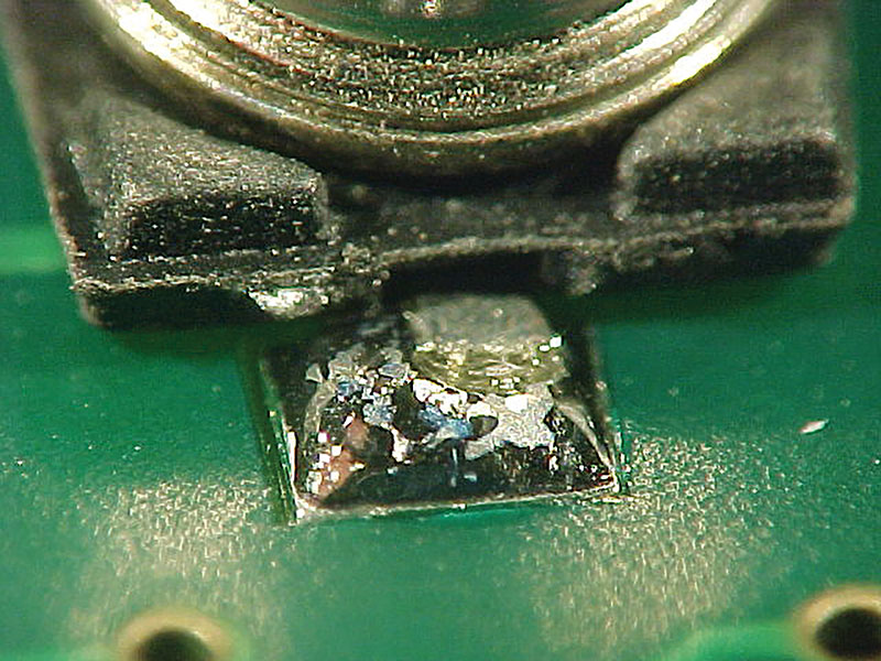
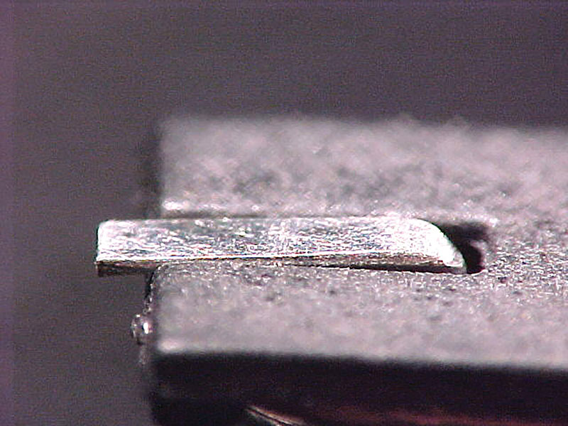
FIGURE 1 shows the lead to be floating in the solder joint, suggesting poor wetting. When we examine the component lead and plastic body, however, the lead is not parallel, so it always sits off the pad surface, even if perfectly soldered. The lead sits in a cavity in the component body to maintain its position. But with the size of the pad used in the design and a full solder paste print, the component body will always lift.
To continue reading, please log in or register using the link in the upper right corner of the page.
{!guest}


Figure 1. The lead at the top appears to show poor wetting, but the pad design is such that the pin is not parallel to the component body.
To improve the component, the position of the pin should be parallel with the body. Ideally the opening of the body of the lead should be wider or angled to permit solder to wet without lifting the part. A simple shop-floor fix is to order another stencil and reduce the width of the paste print, decreasing the lift during reflow.
We have presented live process defect clinics at exhibitions all over the world. Many of our Defect of the Month videos are available online at youtube.com/user/mrbobwillis.
is a process engineering consultant; bob@bobwillis.co.uk. His column appears monthly.
Register now for PCB West, the leading conference and exhibition for the printed circuit board industry! Coming this September to the Santa Clara Convention Center. pcbwest.com


