Dog Ears and Witch Hats

Achieving printing nirvana is largely dependent on solder paste material, print speed and deposit release.
Ahhhhh … screen printing utopia. We process engineers strive for this existence. In a perfect process, printed solder paste would emerge from the stencil as exact replicas of the aperture shape: nice, flat, brick-like deposits. And, while modern printers and advanced materials get us close, solder paste is still, well, solder paste. The materials are not inks; they have a grain structure that is getting smaller in size and distribution and is suspended in flux. Try as we might, with these particles, there will be material undulation at best, and flat paste surfaces will likely never be a certainty.
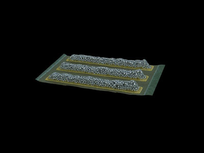
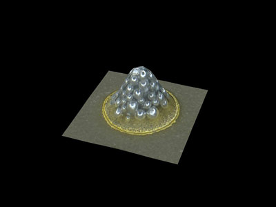
With printing, we must be pragmatic. It’s not a digital process, and many variables come into play. The goal, of course, is to fill all the apertures on the stencil fully with solder paste to obtain the best deposit shape and volume possible. This is easier said than done, as the range of aperture sizes across a stencil can be broad, with 1mm square, 300µm and 200µm openings next to one another. Each of those apertures – from the very large to the very small – must be filled. Since printing with different thickness stencils is a nonstarter (generally and practically speaking), compromise is required, and that challenges our utopian ideal. Squeegee pressure, stencil thickness, print speed and separation speed must be balanced to accommodate variations in required deposit sizes. When all inputs aren’t optimized and in perfect balance, solder deposit shape differences can have the potential to introduce process problems. Known in the printing world as “dog ears” on square or rectangular deposits and “witch hats” on circular deposits (FIGURE 1), these solder paste deposit peaks may be defect bugbears, especially in the world of high-density, miniaturized assemblies.


Figure 1. Solder paste peaks of dog ears (left) and witch hats (right) may seem benign if the material volume and location are correct, but they can be problematic in certain circumstances.
Like-minded process engineers out there, however, may be asking if these small peaks really matter. After all, provided solder paste is deposited in the right volume, in the right place, at the right time, then the outcome should be acceptable. Assuming the printing machine is running at the right speed and process pace (the right time), and the SPI machine verifies the proper location (the right place) and quantity (the right volume), then what problems could these small peaks really cause? Depending on the size and location of the dog ears and witch hats, these seemingly inconsequential paste misshapes may contribute to defects – both in placement and reflow. Very small components like 01005s, for example, may skew during placement if the paste peak is too high. While one edge of the component is seated in the paste, a dog ear may prevent the opposite end from being positioned properly. Additionally, with very large material peaks, paste may be dislodged during subsequent processing and cause bridging during reflow.
Preventing dog ears and witch hats from occurring depends largely on the solder paste material, print speed and deposit release from the aperture. So, keeping other variables in balance, what is the best approach to try to minimize these shape abnormalities? Not surprisingly, there are many factors and multiple approaches to consider, depending on the assembly being produced. Here are some probable fixes:
Separation speed and distance. Stencil separation speed can influence the number of dog ear and witch hat occurrences. Some materials adapt better to a fast release, some to a slow release. My general rule of thumb is if using a fast printing paste (>150mm/sec.), release the stencil quickly (20mm/sec.). With a slow printing paste (between 50mm/sec. and 70mm/sec.), a slower release (5mm – 10mm/sec.) is advised.
Solder paste. Some solder pastes are just more prone to these peaks than others, so try a new material. While solder requalification is quite an undertaking, leverage a significant product or process change as an opportunity to initiate a material evaluation.
Stencils/stencil coatings. If solder paste gets stuck in the corners of the aperture, it can pull paste up on release due to surface tension and cause material peaks. Using a stencil coating inside the apertures can encourage a more uniform release. Of course, the release characteristics also come down to the stencil manufacture quality, the type of stainless steel used (standard or fine grain) and stencil tension integrity, so be sure to evaluate these factors too.
Changing the aperture shape. Putting radii in a rectangular or square aperture can encourage a cleaner release. This adjustment minimizes the tendency of material to stick in the corners of the aperture, which is where the highest surface tension is present. Suggest your stencil manufacturer provide 20µm radii corners. It may reduce dog ear or witch hat occurrences.
Printing is a challenging process and getting increasingly more demanding with modern board designs. It’s not enough to rely on SPI data alone, and, often, good old-fashioned process engineering insight is required.
is global applied process engineering manager at ASM Assembly Systems, Printing Solutions Division (asmpt.com); clive.ashmore@asmpt.com. His column appears bimonthly.


