The Boundary Scan Toolbox

Enabling embedded and other value-added test in your toolbox.
The popularity of boundary scan (IEEE 1149.1) has been increasing through the years to become one of the preferred methods of electronics manufacturing testing of printed circuit board assemblies. Boundary scan is commonly used as a limited access solution for high-node-count PCBAs (10,000 to 20,000 nodes). Due to component density on board, it is typically either not possible or too costly to test such PCBAs using in-circuit test (ICT) bed-of-nails solutions.
Over the years, the typical boundary scan toolbox has expanded to include shorts testing, voltage measurement testing, Cover-Extend, embedded BIST (built-in self-test) and Intel Silicon View Technology.
Structural shorts test. The integrated boundary scan toolbox is not a substitute for an ICT shorts and opens test, which can detect shorts for all accessible nodes. However, boundary scan offers the ability to selectively check for a possible short by measuring the resistance between power nodes, where a short will cause a catastrophic failure (FIGURE 1) to a PCB when the circuit board is powered on. This is a very welcome addition for manufacturing test folks who need to avoid costly damage to the PCBA.
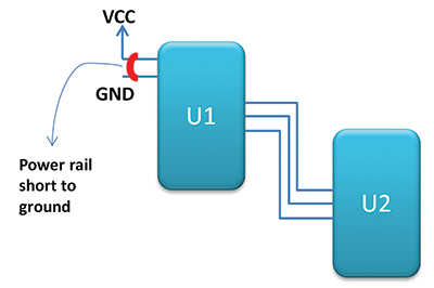
Figure 1. Catastrophic short.
Voltage measurement. Ensuring the correct power-up voltage for the PCBA is another important part of the boundary scan toolbox. This measurement ensures the boundary scan test will not fail due to inadequate voltage levels of the boundary scan devices, something that can be hard to diagnose, as the test engineer will not get a straightforward failure message to indicate that a power rail is faulty.
Nowadays the manufacturing test engineer can integrate a power supply and a low-cost multifunction switch/measurement instrument into a boundary scan tool. Using the built-in software control interface, the engineer can take control of the power on/off and have the ability to measure the resistance and voltage of the power rail on board (FIGURE 2).
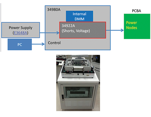
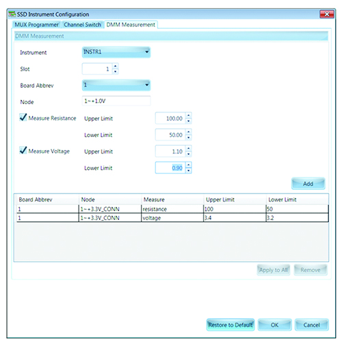
Figure 2. Hardware and software enhancement that enables resistance and voltage measurement.
Cover-Extend Technology. CET is a hybrid between VTEP (vectorless test enhanced performance) and boundary scan (FIGURE 3). It enhances the overall capability of the boundary scan tool by enabling structural tests on non-boundary scan devices such as connectors that are connected to a boundary scan device. The technology works as follows:
- The VTEP sensor, which capacitively picks up stimulus signals, is placed on the component to be tested (e.g., a connector).
- Traditional VTEP methodology required physical test access (e.g., test probes) to deliver this stimulus signal. However, with Cover-Extend, the stimulus signal is delivered via a boundary scan device.
- Per the IEEE 1149.1 standard, using only the test access port, the Cover-Extend test can deliver the necessary stimulus signal to the connector.
- A defect (e.g., an open) on the path between the boundary scan device and the VTEP sensor will affect the stimulus signal that is bound for the sensor.
- The result is captured and diagnosed by the boundary scan software tool; thus the defect is detected.
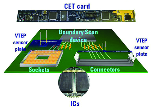
Figure 3. Cover-Extend technology.
Embedded test (BIST and Intel SVT). Built-in self-test (BIST) has been gaining ground in the industry with the recent passing of the IEEE 1149.1 2013 and IEEE 1687 standards, both of which support embedded testing. BIST has been around for some time, but had been mostly implemented only at the chip level. Implementation of on-board test was not widespread, mainly due to limited availability of BIST support at the board level from boundary scan device vendors. Since then, boundary scan tools have included STAPL/SVF to enable support on various devices with instruction “opcodes” for BIST testing (FIGURE 4).
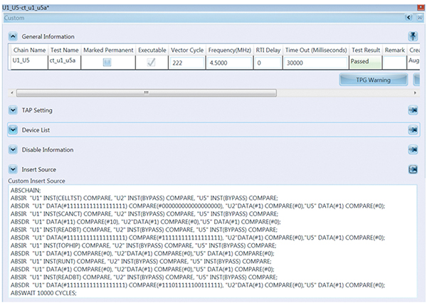
Figure 4. Boundary scan tool interface that supports STAPL/SVF.
Intel Silicon View Technology is another big boon for embedded testing, as it permits further integration of boundary scan tools. SVT enables tests for Intel Haswell CPU designs in situations where test access is constrained by tight PCBA real estate or high-speed signal fidelity.
It requires test access to the debug port 2 and uses Intel DFx Abstraction Layer (Intel DAL) to securely access the Haswell CPU silicon to verify its function and that of surrounding devices.
Intel SVT requires the BIOS to be set up according to Intel BIOS Writer Guide3, reserving a designated register to host the results of the Intel SVT test. During manufacturing test, the PCBA under test has to be powered up safely to run the BIOS, and Intel SVT will post the results of its test into the designated register. The content of the register is then compared to known good board values to assess whether the PCBA passes or fails the set of tests.
Intel SVT will test the following via the Haswell CPU (and BIOS):
- Platform hub controller (PCH).
- Memory.
- Graphics, e.g., VGA, HDMI, eDP.
- High-speed I/O(HSIO), e.g., PCIe, SATA, USB3.
- Communication interfaces, e.g., LAN, USB2.
- I/O peripherals, e.g., keyboard, audio.
Continued advancement of both software and hardware in the boundary scan toolbox and concurrent development and support of industry standards will help to regain test coverage lost on traditional ICT methods. In the near future, the handy boundary scan toolbox is likely to expand with new features to exceed the expected test coverage of today’s complex PCB assemblies.
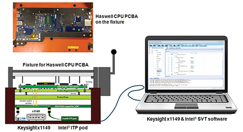
Figure 5. Small footprint solution comprising a Haswell CPU PCBA fixture, Intel ITP pod, x1149 boundary scan analyzer and software on a Windows 7 PC.
is a technical marketing engineer at Keysight Technologies (keysight.com); jun_balangue@keysight.com. The former Agilent Technologies Electronic Measurement Group is now Keysight.


