When Boundary Scan Hits Roadblocks

Every test strategy has its challenges. Suggestions on how to cope with programming issues.
The IEEE 1149.1 standard, commonly known as boundary scan, is a well-adopted electronics manufacturing test strategy used throughout the lifecycle of a printed circuit board assembly – from prototypes, new product introduction builds, production runs and functional tests, to field repair. It is a low cost, yet effective tool for capturing structural defects during manufacturing.
While boundary scan is widely adopted, challenges are bound to happen during the implementation phase that will frustrate test and design engineers. These challenges can crop up in various situations: for example, during boundary scan implementation on IC devices, wrong boundary scan description language (BSDL) declaration that does not match the actual device, poorly designed PCBA test for boundary scan, or during implementation of the various boundary scan tools and integration to other manufacturing test strategies.
Boundary scan implementation at IC level. Boundary scan is mostly implemented for high pin count IC devices such as CPUs, ASICs and FPGAs, where the devices are designed with boundary register cells, test access ports (TAPs) and instruction registers (FIGURE 1) to facilitate boundary scan testing.
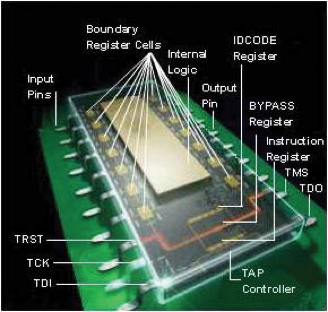
Figure 1. Integrated circuit device with boundary scan implemented in the silicon.
Various causes may result in the boundary scan implementation at the IC level running into roadblocks. Let’s take a closer look at some of these potential pitfalls:
- Single control cell on data bus, address and control pins (CAS, RAS, CS and WP) (see FIGURE 2 for the BSDL). When performing Silicon Nail test for memory devices such as DDRs (with the CPU as the upstream boundary scan device), the Write and Read operations are executed to the target devices. With a single Control cell for all the DDR data, address and control pins, it will mean that at any one time the DDR interfaces are all either driving or receiving signals. This will cause a failure for the Silicon Nail test implementation because during the Read operation, the Control pins and Address lines of the DDR need to be driven from upstream boundary scan devices (CPU, ASIC , FPGA), while the DDR Data lines need to be received by the CPU. The single control cell will not allow both driving and receiving to occur simultaneously.
- Sensitive pins of an IC device with boundary scan should not to be controlled and should preferably be made “internal.” Exposing them even as an “observe only” function in the BSDL will sometimes lead to undesirable behavior and cause the test to be unstable.
- The most common stumbling block happens during boundary scan initialization. Under the IEEE 1149.1 standard, the IC device should enter boundary scan mode upon power up. Often, some devices, such as CPUs and ASICs, may need sequencing for a few signal pins in a specific order for the device to successfully enter into boundary scan mode. If the device used in the PCBA was not designed to enable the special signals to be controlled, then the device will not be able to enter into boundary scan mode.
- Challenges in the IEEE 1149.6 standard implementation for testing the differential pins. In some cases, the boundary scan device needs to be initialized to program the hysteresis voltage of the differential receiver to sense the low (0) and high (1) signals to achieve a stable 1149.6 test.
- Challenges in the IEEE 1149.6 implementation of detecting a shorted capacitor between the differential driver and receiver pins. Most boundary scan devices do not include the mandated DC extest instruction on testing differential pins capacitor. In order to resolve the challenges, the boundary scan device should implement the DC extest instruction to effectively capture shorts on capacitors in between differential driver and receiver.
- Wrong placement of test access port (TAP) pins (TCK, TMS, TDI, TDO and optional TRST) will cause a possible short during manufacturing test that is hard to debug (FIGURE 3).
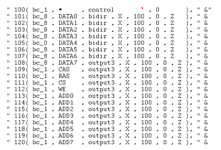
Figure 2. BSDL with a single control cell (100) for all the DDR address, data, and control pins.
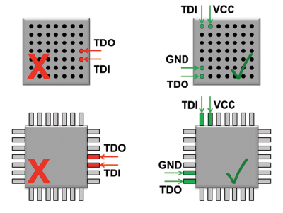
Figure 3. Placement of TAP pins for manufacturing and better signal integrity.
-
- For better structural testing and signal integrity, place the TAP pins at the end or the corner of a package to reduce the likelihood of being bridged by the solder.
- Where possible, place power or ground pins between TDI, TDO and other TAP signal pins.
Boundary scan description language (BSDL). Next, let’s look at some reasons why roadblocks may arise from the BSDL:
- The details entered into the BSDL do not match the actual boundary scan cell and registers in the silicon. BSDL verification against the silicon is a critical part of the process, and the final BSDL should be strictly updated in order for the boundary scan implementation at board level to be successful.
- Based on specific design scenarios, the compliance pins may be related to enable the boundary register, and not the TAP operation. In such cases, the integrity, IDCODE and bypass tests may pass, but the boundary register (BReg) test would fail.
- Compliance pins and design warning not documented in the BSDL.
- Using the BSDL file to alert test engineers.
- Sometimes, cell orders are changed during silicon revisions, and these may lead to incompatible BSDL files for production boards that may have a mix of old and new chip revisions. Supporting a test in such cases may be difficult due to incompatibility between BSDLs.
- Not adhering to IEEE 1149.1/1149.6 standards.
Board design for test (DfT). Several considerations must be kept in mind to ensure design-for-test guidelines are followed during the board design phase to avoid hiccups during boundary scan tests for these boards.
- Control of compliance pins for boundary scan entry of a device is a very tricky affair. Often, when there is a functional logic like a CPLD or an FPGA, compliance pins should be treated with care during an image revision of these programmable devices. Any oversight to controlling the correct state of the compliance pins during an update may result in malfunctioning of the boundary scan program.
- While designing boundary scan chains for a new device, it is good practice to understand the IO characteristics of the TAP signals. Any oversight in knowing that a TDO is an open drain IO may result in the device not functioning unless it is reworked. Read the specs thoroughly while performing board DfT, which may consist of a new device used.
- Post silicon errors in the boundary scan compliant behavior of ASICs could be a challenge to handle. When such devices are chained with no easy option to bypass them on the board, the workaround could be painful. But here’s a possible workaround: If unclear whether boundary scan works on a device, add a jumper, R1, after TDO then add another jumper, R2, in parallel between TDI and TDO across the boundary scan device and R1, but keep it unloaded (FIGURE 4). To bypass U2, remove R1 and install a jumper at R2. This permits the bypass of U2, even if the boundary scan mode is not working.
- In the event of unstable boundary scan chain test – e.g., fan-out issues in long chains – use buffers at the TAP signals (TCK, TMS & TRST) to eliminate fan-out issues. The guideline is to assign a buffer after three to four devices in the chain (FIGURE 5).
- Enable or disable pins on upstream components that should have test access assigned to them or connected into a boundary scan output cell. This permits the boundary scan tool to disable the upstream device during testing.
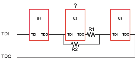
Figure 4. Bypass DFT during prototype.
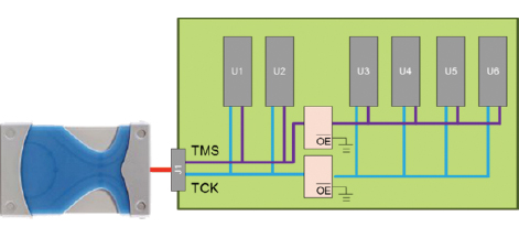
Figure 5. TAP buffer for long chains.
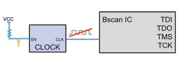
Figure 6. Disabling clock of upstream devices.
There will always be challenges in every test strategy, including boundary scan. The key is how to put a process in place in the PCBA production cycle to ensure the possibility of a non-working or unstable boundary scan test is minimized or completely eliminated during production testing.
is a technical marketing engineer at Keysight Technologies (keysight.com); jun_balangue@keysight.com.


