CT – 3-D X-ray Analysis
 CT takes time, but can virtually microsection and analyze any plane in an entire sample.
2-D offline x-ray inspection of electronics is directly analogous to 2-D medical x-ray imaging, the only difference being image magnification is required to see the much smaller features within electronic devices and boards. (Also, the sample doesn’t talk back!) Medical x-ray imaging also offers CT scanning (also known as 3-D x-ray or computer tomography or CAT scans), and the same technique is available for electronics analysis. From Greek, tomography means writing slices.
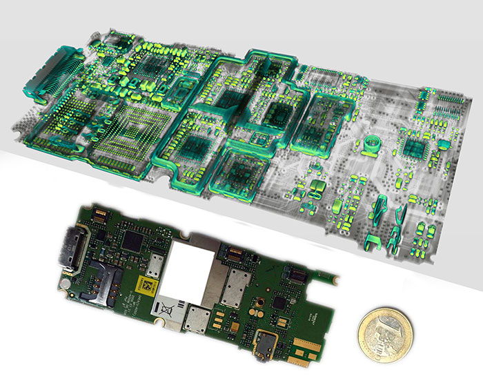
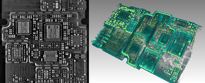
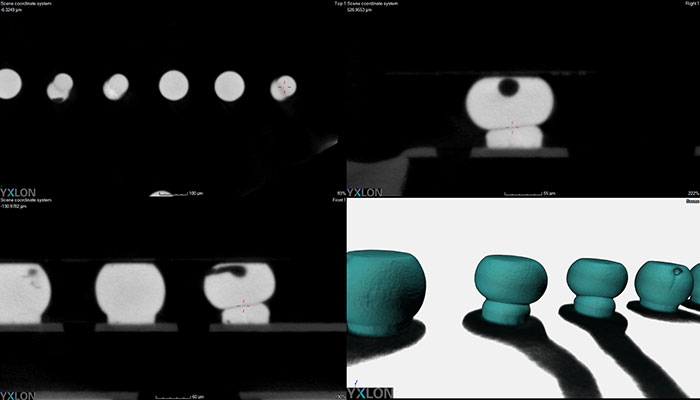
CT provides a 3-D density map model of the sample from which virtual 2-D x-ray slices can be taken and examined in any plane within the model. Consider it like being able to take virtual microsections anywhere, at any angle and as often and repeatedly as desired through the sample without having to cut, pot, polish, optically image, repolish, re-image, etc., as when making a traditional microsection. 3-D representations of the sample may also be created and virtually sliced (FIGURES 1 to 3).

Figure 1. Helical CT scan of example cellphone board.

Figure 2. Circular (cone beam) CT scan of a section of the cellphone board in Figure 1. A virtual 2-D x-ray slice of a single level in the z-plane (depth) of the board is shown (l). Voiding under the QFNs can be seen without packaging or second-side components obscuring the view.

Figure 3. CT analysis of 80µm diameter microbump with head-on-pillow defect. Virtual 2-D slices in the x, y and z planes are shown together with a 3-D rendered view.
Whether the sample is a person or a circuit board/component, CT requires three distinct stages to be undertaken. These are 2-D x-ray image acquisition, 3-D model reconstruction, and 3-D model visualization and analysis.
X-ray image acquisition requires a self-consistent set of many 2-D x-ray images to be taken, ideally from 360° around the sample. Features within the sample must not move relative to each over the image acquisition. This is the reason patients in hospitals remain “fixed,” and the x-ray tube and detector rotate around them – that’s what’s inside the circle they go into. For electronics CT, where typically internal features do not move around, we can keep the tube and detector fixed for imaging and rotate the sample in a precise way. CT functionality can be provided as an option for some offline 2-D x-ray systems. However, the typical vertical arrangement of tube and detector means CT results are good, but not optimal, as the sample rotates horizontally, which can allow unwanted movement of the sample during acquisition, particularly for larger samples. Alternatively, if CT analysis is your primary workload, then crossover CT systems from those used in nondestructive testing (NDT) environments may be worth considering. In these systems the tube/detector axis is horizontal, and the (larger) sample can be more accurately rotated in the vertical plane.
Image acquisition takes the most time to complete. The time depends on the number of images taken and the image averaging, if any, applied to each image.
More images and longer image averaging, providing a better signal-to-noise ratio in each image, gives better information for the model. But it takes more time.
Compromising and shortening this process does give results, but is it sufficient to see what you need at an acceptable level?
Reconstruction takes the acquired 2-D images and inserts them into a mathematical algorithm from which the 3-D model is created. This is a highly computationally intensive operation. Consider there may be many hundreds of 2-D x-ray images, each containing megapixels of information. The reconstruction algorithm generates a 3-D density map of all the features within the sample from all the images. The most commonly used reconstruction algorithms for electronics are based on the Feldkamp method (aka Feldkamp, Davis & Kress, or FDK, cone beam CT or circular scan CT).
Up until as few as 10 years ago, reconstruction was not a quick process, as the available computational resource was much more limited, typically to custom hardware rather than using PCs. However, the rapid development of GPUs contained within modestly priced, commercially available graphics cards for PC gaming now provides ready access to massive computational power on a high-end desktop PC. This has not only dramatically reduced reconstruction times but offered new paradigms for reconstruction methodology. This transforms the opportunities for CT, in my opinion. It now allows, I believe, better and more computationally hungry CT reconstruction algorithms to be used for electronics. The Feldkamp/cone beam method has been a good compromise to provide reasonable CT models on the historically available computing hardware. It works well but could not be said to be the best, as there are some underlying technical issues, such as artefact generation. Newer reconstruction algorithms for electronics, such as helical CT, can remove these flaws. In helical CT, the sample rotates, as for cone beam CT, but the tube and detector also move vertically with respect to the sample. In this way the image acquisition is taken over a helix rather than a circle.
Whichever reconstruction method is used, the result is a 3-D model containing a density distribution of the materials within the sample. The model is made up of a three-dimensional array of volume pixels, or voxels, that can be 1024 x 1024 x 1024 elements in size, or larger. Visualization of the model, therefore, requires special software (and the GPUs again) to handle this vast amount of data, yet enables virtual “dicing and slicing” and 3-D rendering for optimum analysis (Figures 1 to 3). Remember, the virtual 2-D slices are not the original x-ray images but reconstructed views from the original data. For example, you can easily select different layers in the depth of a board to check the voiding at different locations in a device, such as at a die interface and at a substrate interface, without the view being obscured by other layers or features.
It should be noted the small feature sizes in electronics require high image magnification. This means the sample needs to get close to the x-ray tube, yet still be able to rotate freely. Therefore, the best resolution CT results for the smallest electronic features may require cutting down the sample so it gets closer to the tube and provides the necessary magnification. In these situations, consider CT as the step before a full microsection. You have already committed to cutting the sample into the epoxy, but before you do, CT offers a method to virtually microsection and analyze at any plane in the entire sample ahead of preparing (if necessary) what you hope is the correct slice for the microscope.
CT offers the potential of a lot of additional information. It takes time and may require cutting the sample, but access to huge, low-cost number-crunching power means, I believe, more opportunities from CT and related technologies will be coming to electronics in the future.
Au.: Images courtesy René Sommer of Yxlon International.
, is an expert in use and analysis of 2D and 3D (CT) x-ray inspection techniques for electronics; dbc@bernard.abel.co.uk.


