

Defect of the Month

A look at solder mask contamination on pads.
This month we look at solder mask contamination on pads. FIGURE 1 is a very, very bad example that never should have made it to the customer. Solder mask residues are visible on the surface and around the edge of the pad. There is also a level of solder mask undercutting.
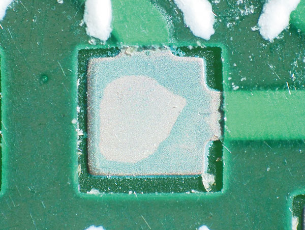
FIGURE 1. Solder mask residues.
This would not be acceptable per any standard and would have shown complete nonwetting during soldering. This would have led to a bad day in the office for the assembly engineer or, more important, the shop floor staff.
We have presented live process defect clinics at exhibitions all over the world. Many of our Defect of the Month videos are available online at youtube.com/user/mrbobwillis. Find out how you can share our new series of Defect of the Month videos to explain some of the dos and don’ts with your customers via CIRCUITS ASSEMBLY: https://bit.ly/3mfunlF.
is a process engineering consultant; bob@bobwillis.co.uk. His column appears monthly.
X-ray can’t catch all failures.
This month we we look at solder joint separation from pads with dye and pry testing, which is of course intended, and in FIGURE 1 shown as a perfectly good solder joint. (Well, until I covered it with dye and broke it, that is.)
To continue reading, please log in or register using the link in the upper right corner of the page.
Get agreement on what constitutes “rework” – and a capable operator.
This month we look at etching defects and their removal – or presence, as in the case of FIGURE 1. A customer was surprised to find a batch of bare boards with this level of rework.
To continue reading, please log in or register using the link in the upper right corner of the page.
Getting a close-up look at board quality.
A printed board microsection is one of the best ways to examine the quality of boards and any faults or failures.
The microsection (FIGURE 1) shows a plated through-hole that has been soldered with the nickel layer and through-hole copper visible. Normally, customers would accept the plating standards offered by the fabricator, or define their own, which may or may not impact the price. The nickel layer is part of the nickel/gold surface finish with the very thin gold of less than 1µm consumed during soldering and not visible. The remaining nickel is 5µm, and the copper is around 32µm. This is generous on many circuits board produced today and soldered very easily in production.
To continue reading, please log in or register using the link in the upper right corner of the page.
When separation occurs, check the oven settings.
This month we look at printed circuit board delamination. As FIGURE 1 shows, delamination is barely visible on the surface of the board and confined to the area around through-holes and where the solder mask is cracking.
To continue reading, please log in or register using the link in the upper right corner of the page.
Is the board preheat process optimized?
This month we look at incomplete fill of plated through-holes. During any soldering operation a balance of flux and solder/paste chemistry and soldering temperatures creates good and reliable joints. In FIGURE 1 the solder has not filled the hole completely but still exceeds the requirements of IPC-A-610, class 2 of 50%; measured, it may be 75% filled.
To continue reading, please log in or register using the link in the upper right corner of the page.

Press Releases
- SMTXTRA Partners with Quantum Systems to Expand Representation in Key Territories
- KYZEN Announces Exclusive Partnership with Manufacturers’ Representative Restronics Florida
- Koh Young will Showcase its Award-winning Inspection Solutions at SMTconnect with SmartRep in Hall 4A.225 on 11-13 June 2024 in Nuremberg, Germany
- Precision Automation & Assembly Appointed as New England Rep for Kubler US