

Forefront
 Government-funded organization hopes to knock down barriers to commercialization.
The American Vacuum Society (AVS) held its annual conference in Portland, OR, with roughly 2,000 in attendance for the November meeting. The conference included many technical presentations by students, faculty and industry on cutting-edge issues associated with materials, processing and interfaces.
Among the highlights this year was a special session on the Chips Act. The session on the Chips and Science Act Implementation for Microelectronics (including workforce) was moderated by Dr. Alain Diebold, SUNY Polytechnic Institute, and Dr. Tina Kaarsberg, US Dept. of Energy Advanced Manufacturing Office.
The first invited talk was given by Dr. Jay Lewis, director, National Semiconductor Technology Center (NSTC). NSTC is a public/private consortium authorized and funded by the US government to serve as the focal point for research and engineering throughout the semiconductor ecosystem, advancing and enabling disruptive innovation to provide US leadership in the industries of the future. Dr. Lewis announced the incorporation of a new nonprofit entity, SemiUS, to operate the NSTC. SemiUS will work in partnership with the US Department of Commerce to develop and implement a wide variety of programs to fulfill the mission of the NSTC consortium. The focus is on building a strong semiconductor research and development ecosystem in the United States.
ECTC revealed the latest developments in 3-D hybrid bonding.
More than 50 presentations on hybrid bonding filled rooms to capacity at the IEEE Electronics Components and Technology Conference (ECTC) in Orlando, as did the Tuesday morning panel session. That panel discussion, on "Copper Hybrid Bond Interconnections for Chip-to-Wafer Applications," organized by Infinera and Qualcomm and moderated by TechSearch International, included perspectives from design and EDA (Synopsys) and research institute IMEC, users of hybrid bonding (AMD with production at TSMC and Intel with its internal development program), equipment makers Besi and EVG, and yield and reliability specialist PDF Solutions.
Synopsys pointed out the importance of design tools and IMEC described key drivers for 2.5-D and 3-D integration technologies such as increasing system complexity, increasing need for heterogeneous integration, increasing die-to-die interconnect data bandwidth (more interconnect channels and higher interconnect speeds per interconnect), reducing die-to-die interconnect energy with shorter distance interconnect, scaled, lower capacitance interconnects, and lower voltage. IMEC noted the issue is not the number of interconnects but rather the available (local) interconnect density enabled by interconnect pitch scaling. Many of today's hybrid bonding applications using die-to-wafer structures are focused on the high-performance space where the cost can be justified, including stacking SRAM cache and logic-on-logic, as introduced by AMD's products in desktop, servers, and AI/machine learning.

Large crowds mulled the latest substrate trends and new developments in 3-D IC hybrid bonding.
The IEEE Electronics Components and Technology Conference (ECTC) returned to an in-person conference at the end of May with more than 1,500 attendees, domestic and international. Attendance in San Diego matched pre-pandemic numbers. While some presentations remained virtual, using video recording, many were onsite. A variety of electronics packaging topics were discussed. Judging by the crowded rooms, this year’s hot topic was 3-D IC hybrid bonding.
Advanced packaging. A pre-conference Heterogeneous Integration Roadmap workshop discussed trends in networking for the future and new developments in advanced packaging for high-performance computing and data centers. The workshop concluded with a panel of presenters discussing the latest trends in medical health and wearables.
Plenary sessions covered some of the latest topics. The MicroLED display session focused on high-volume manufacturing progress and challenges. In a session on the evolution of IC substrate technology, panelists from Intel, Amkor, Ajinomoto, AT&S and Atotech discussed the latest substrate trends.
The special session – Meeting Next Generation Packaging Challenges from Chiplets to Co-packaged Optics – included panelists from AMD, Cisco, Marvell and Synopsys (FIGURE 1). Panelists discussed the importance of co-design and changing the approach to design, including system-level design. The combination of digital and photonics is coming. Integrating this in 3-D will include the laser, modulator, filters and detectors. Interfaces and the design platform are important for robust manufacturing, including product quality, debug and traceability, and in-field optimization. The panel concluded that, with increased use of chiplets, continued work is required in the areas of test and known good die (KGD), thermals, power deliver and system-level integrity. Adoption of standards such as the recently introduced UCIe is important to align the industry around an open platform to enable chiplet-based solutions. Thermal management remains one of the major bottlenecks with 3-D.
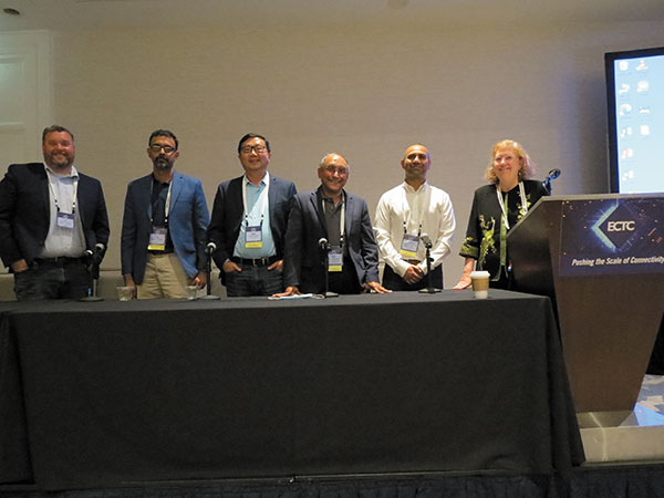
FIGURE 1. A special panel on packaging challenges. Panelists included (from left) Kevin O’Buckley (Marvell), Raja Swaminathan (AMD), Ming Zhang (Synopsys), Ravi Mahajan (Intel), Sandeep Razdan (Cisco Systems), and moderator Jan Vardaman (TechSearch).
A special night session focused on the US Department of Defense (DoD) in the state-of-the-art heterogeneous integration (SHIP) program. The opening statement from the office of the Undersecretary of Defense for Research and Engineering explained the backdrop of the program. Speakers from Intel and Qorvo, recipients of US government funding, described their activities. Qorvo is focused on RF, and Intel is focused on high-performance computing with its embedded multi-die bridge (EMIB) technology. The panel admitted that, in the absence of a volume supplier of buildup substrates, the DoD depends on a global substrate procurement strategy.
A session on diversity and career growth provided advice from a panel of experts, including representatives from IBM, Lam Research, Edwards and Cadence. The plenary session covered digital transformation with participation from Intel, TSMC, Yole, Onto Innovation and Samsung. A late-night session focused on Interconnect Technologies for Chiplets with participants from Intel, IBM, Unimicron, TSMC, SPIL and Furukawa Electric. Participants from Taiwan and Japan dialed into the session to discuss topics including embedded bridge, the incorporation of memory in advanced package developments in optical packaging, 3-D packaging and substrates.
Adapting to substrate shortages. With the continued substrate shortage, companies focused on the potential for a fan-out wafer level package (FO-WLP). Numerous presentations covered several options, with new applications for fan-out discussed. SK Hynix discussed the potential for memory applications. IME A*Star discussed FO-WLP antenna-in-package (AiP) for automotive radar applications. Researchers at UCLA described their work on FO for micro displays. RFcore discussed FO-AiP for 5G mmWave applications. Amkor, ASE and Samsung presented package options for FO-WLP.
Processing FO in a panel has been proposed as a way to lower the cost by increasing the number of parts with large-area processing. Fraunhofer and the Technical University of Berlin discussed the technology limits of panel processing, describing warpage and die shift as the major issues. Layout adaptation is promoted to overcome die-shift challenges on large panels. Samsung Electronics discussed the reliability of the via structure in its FOPLP line. Amkor introduced its 650mm x 650mm panel line. Nepes provided reliability data on FO packages fabricated on its new panel line based on Deca M-Series technology (FIGURE 2). Deca Technologies described 20µm device pad pitch with its M-Series process. The use of adaptive patterning provides a way to handle die shift. Dai Nippon Printing introduced its panel-based RDL interposer with a 2µm pitch semi-adaptive process for chiplet integration.
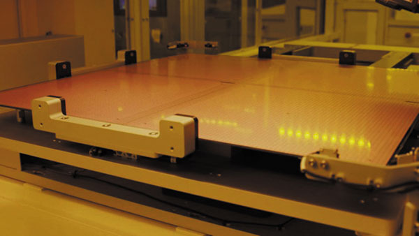
FIGURE 2. The Nepes nPLP 600mm x 600mm fanout panel line reportedly can produce five times as many chips as one 300mm round panel.
Several presentations focused on new substrate options, including glass as a substrate and RDL interposers. Developments in glass substrates were introduced with papers from Korea Electronics Technology Institute and Georgia Tech. TSMC introduced its organic interposer CoWoS-R+ technology that replaces the silicon interposer with an RDL structure. The plus indicates the integration of a large amount of high-density integrated passive devices (IPDs) that serve as decoupling capacitors. The integrated de-cap capacitors suppress the power domain noise and enhance HBM3 signal integrity at a high data rate. Optional silicon connection blocks (bridges) provide high-density die-to-die connections. IBM provided updated work on its direct bonded heterogeneous integration (DBHi) silicon-bridge package, in which the Si bridge is connected to the die and then mounted on the laminate substrate. SPIL provided recent reliability data for its embedded bridge package. Unimicron discussed its hybrid substrate with a buildup film.
3-D hybrid bonding. Three years ago, many ECTC papers focused on R&D activities in hybrid bonding. This year, more than 30 papers discussed hybrid bonding process improvements and new developments. While image sensors have been using hybrid bonding for many years, Sony described their recent work to develop 1µm face-to-face bonding and a new thinning process that minimizes Si thickness variation across the wafer. Adeia’s (formerly Xperi) study of the influence of Cu microstructure on the thermal budget shows the possibility of a 20° to 40° reduction in the final anneal temperature. CEA-Leti presented research conducted with Intel on a new die-to-wafer (D2W) collective bonding self-assembly process using water droplets with high alignment accuracy and high throughput. SK Hynix reported the work on wafer-to-wafer (W2S) DRAM stacking for DRAM. Samsung presented several papers on hybrid bonding, including research on controlling bonding voids. AMD described its V-Cache, now in commercial production for servers, desktops and gaming, using TSMC’s SoIC process. TSMC described an extension of its SoIC process.
Co-packaged optics. Several presentations focused on co-packaged optics (CPO). Rockley Photonics introduced a fan-out silicon photonics module for next-generation CPO. Rain Tree and IME A*STAR described a heterogeneous integration package using FO-WLP for a hyperscale data center. IBM Canada, GlobalFoundries and others discussed optical fiber pigtail integration for CPO. Cisco described its vision for CPO and challenges in the use of through-silicon vias, including high warpage, optical fiber coupling, and chip-on-substrate assembly. Reliability requirements were also highlighted. A joint paper from EV Group, Tyndall National Institute, IMEC and Ghent University described a high-speed Si photonic switch with a micro-transfer-printed III-V amplifier. ASE described its CPO assembly.
Emerging areas. Presentations also covered additive manufacturing, 3-D printing, developments in packaging and assembly for wearables, and micro LEDs.
Next year’s ECTC will be held in Orlando May 30 to Jun. 2.
is president of TechSearch International (techsearchinc.com); jan@techsearchinc.com.
Can we build on past successes of cost and task sharing?
Much attention is focused on the importance of boosting electronics manufacturing in the US, but in a recent interview, Emmanuel Sabonnadiere, CEO of CEA-Leti, called R&D the roots of the tree of manufacturing. What a great analogy. Without successful R&D in the electronics industry, successful manufacturing is not possible. Creating the best ecosystem to foster R&D is key.
To continue reading, please log in or register using the link in the upper right corner of the page.

Press Releases
- Bimos Welcomes Z TECH SERVICES as Newest Representative
- Indium Corporation Expert to Present on Pb-Free Solder for Die-Attach in Discrete Power Applications
- Seika Machinery Holds 30th Anniversary Celebration at 2024 IPC APEX EXPO
- StenTech Expands Sales Representation to Enhance Service in Critical Industry Territories