

Current Issue
01005: Size Does Matter
Is it worthwhile to design PCBs with 01005 components? If yes, how so?
I was approached by the vice president of R&D from a high-tech company that develops a wearable mobile accessory. “This is a product with great potential that could be in any household in the world,” he said with enthusiasm. “It’s a rigid-flex circuit board with a wide range of applications.”
Then he laid before me his great dilemma. “The problem is that the PCB is extremely dense, and we’ll be obliged to relinquish several important functions since there’s simply not enough space on the PCB.” I asked him about the sizes of the passive components used and, after receiving the reply, realized we might have the possibility to fulfill his dream.
The trend in consumer electronics – enabling the insertion of many more functions into smaller components – doesn’t halt at the field of SMT components. The use of electronics in recent years has expanded to a variety of applications and accessories. Mobile accessories that pop up everywhere and the loud buzz all around turning inanimate devices into communicators within the existing Internet infrastructure (the Internet of Things – IoT) force a need for the realization and implementation of many more electronic functions in smaller spaces. To cope with this challenge, the production of smaller components does not suffice. The dependency and connection between the PCB, materials and production processes require an in-depth analysis of the soldering process and the points of failure during the planning and design stage. The manufacturers and designers of these components must work in close cooperation to encounter creative solutions that are nothing less than effective.
The smallest component currently in use is known as an 01005. This is a passive component (resistor, capacitor) possessing extremely small weight and dimensions (FIGURE 1). The device is almost invisible to the naked eye. Its dimensions are 0.4mm in length by 0.2mm in width, with a height that varies from 0.1mm (resistor) to 0.2mm (capacitor). The distance between the pads is 0.13mm (5mils). The component’s weight is 0.04mg!
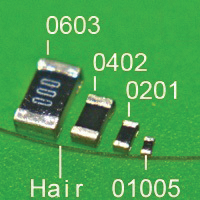
Figure 1. An 01005 component and related larger parts. (Source: FAPS)
An 01005 component’s width and length dimensions are half those of the next larger component, the 0201. In other words, the area of an 01005 is just 25% of that of an 0201. In view of this, an 01005 could be encountered wherever maximum functionality in a minimum area is required. Also, an 01005 has the (very low) weight of only 0.04mg, a mandatory feature in mobile products that are required to be as light as possible. Another very significant advantage of 01005 components is that they can be placed in proximity to the pins of a dense BGA component in order to obtain optimal filtering. When the component under discussion is a dense BGA with a pitch (distance between leads) of 0.5mm or below, 0201 capacitors cannot be placed in between the pins in favor of filtering. An 01005 capacitor, due to its minimal dimensions, can be placed between the pins of a BGA component, thus permitting optimal filtering.
The minimal dimensions of an 01005, and no less important, its weight (0.04mg), result in a number of technical challenges. While they can be machine placed and soldered, it isn’t recommended to work with 01005 components as a default. An attempt should be made, as much as possible within the framework of the PCB area constraints, to design the board using the sequentially larger 0201, which is much simpler and easier to assemble and maintain.
Following are several challenges that may be encountered on designs that use 01005 components:
1. The component is difficult to repair manually. As a result of the component’s tiny area and minimal weight, the 01005 requires special techniques to solder with a soldering iron.1,2
Therefore, it should be taken into account that after soldering the PCB on the automatic SMT line, the component is not likely to be repaired manually. In most instances, if post-soldering repairs or component additions are needed, the manufacturer will have to reassemble the PCB.
2. Extremely accurate application of solder paste is required. One of the most important aspects of successful SMT component soldering is correct application of solder paste. The smaller the part, the more precise the application must be. An ultra-thin (0.25mils) solder mask (stencil) is recommended, and an optimal relationship between the opening (aperture) of the mask’s hole, the mask width, and the solder paste location within the PCB must be ensured.
3. Uniformity of the PCB’s remaining components. Because the component requires accurate and delicate handling during soldering, the remaining components on the PCB must be meticulously selected. The various types of components must be reduced in order to enable uniformity throughout the soldering process. For example, for a circuit board containing an 01005, it isn’t worthwhile to incorporate a large BGA component as well (i.e., BGA component area greater than 25 x 25mm). If not properly profiled, the large thermal mass of the larger component can negatively affect the solderability of the 01005 by causing voiding or other defects.
4. Limited manufacturer options. Due to the advanced technology involved, few manufacturers today are able to successfully assemble 01005 components. Choosing this component will in turn limit the number of EMS companies to select from.
5. Price. The component’s current price is more expensive than the price of larger components in the category – the 0201 or 0402. In coming years, as use of the 01005 increases, the price is expected to become more competitive with those of other components in the market.
High Accuracy Needed
The key to quality assembly of an 01005 component is an accurate application of solder paste. Very accurate application of solder paste must be ensured. The solder paste maximum allowable tolerance is 100µm (0.1mm).
Attention should be paid to several recommendations during the PCB layout process:
- The component’s footprint should be defined according to the component manufacturer’s recommendations.
- The ratio between the stencil aperture for solder paste release and the pad area should be 1:1.
- Release from the solder mask can be defined through a solder mask defined (SMD) or non-solder mask defined (NSMD) configuration. It is necessary to ensure that solder mask is defined in between the pads.
- A minimum distance of 7mils must be maintained between two adjacent 01005 components.
Soldering an 01005 component using an invalid process may result in a substantial number of defects. Common defects in the assembly of 01005 components include:
- Tombstoning. One end of the component may lift from the board during the assembly process (FIGURE 2). This may occur mainly due to deflections in the application of solder paste, or due to inaccurate placement of the component on the pads.
- Bridging (shorts). The component may cling to an adjacent component, creating a short circuit (FIGURE 3). The reason is lack of precision in solder paste application or placement process.
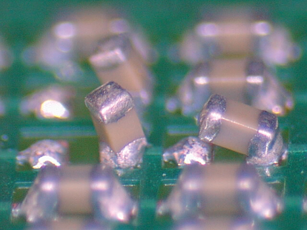
Figure 2. 01005 components are susceptible to tombstoning. (Source: Alpha)
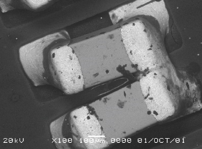
Figure 3. Component bridging is another common defect. (Source: Siemens)
FIGURE 4 shows the proper assembly process of an 01005 component. Figure 4a shows the solder application, Figure 4b the placement process and Figure 4c the reflowed components.
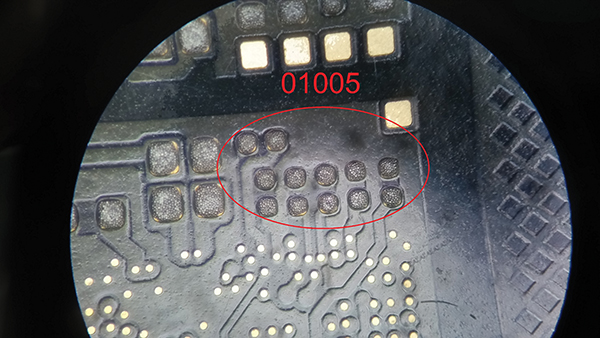
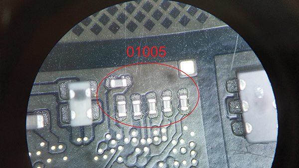
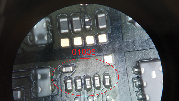
Figure 4. Proper assembly process of an 01005 component. Photographs were taken with microscope using a ratio of 1:40.
There is no question PCBs are becoming denser. An 01005 component, due to its miniature area and weight, may constitute an excellent solution for contending with these challenges. Certainly the component’s soldering requires coping with a number of complex challenges, but by properly defining the component during layout, ensuring a controlled assembly process and mainly an accurate application process, high-quality soldering results can be achieved.
References
1. Brian Czaplicki, “Advanced Rework Technology and Processes for Next Generation Large Area Arrays, 01005, PoP and QFN Devices,” IPC Apex Expo Proceedings, February 2013.
2. Paul Wood and Bob Wettermann, “What You Cannot See Can Be Hand Soldered,” CIRCUITS ASSEMBLY, February 2015.
is vice president of marketing at Nistec Design (nistec.com); arbeln@nistec.com.


