

Current Issue
Advanced Acoustic Methods for Locating Flip Chip Faults
Echoes can reveal otherwise elusive defects beneath the die.
In flip chips, the very small size of structural defects that can generate sudden field failures makes thorough inspection vital. Virtually all structural defects are beneath the die. Acoustic micro imaging (AMI) tools are a practical, nondestructive method for finding and analyzing these defects.
In some flip chips, however, the small size of the flip chip defects and the architecture of the solder bumps can make the defects difficult to discern with standard AMI techniques. This article discusses two AMI techniques that can reveal defects that might otherwise escape notice.
The structural defects that may cause immediate or eventual failure in flip chips tend to occur between the chip and the substrate. These defects – cracks, delaminations and other gap-type features – are the brightest features in images made by acoustic micro imaging tools such as the C-SAM
systems because the anomalies contain an interface between a gas (e.g., air) and a solid (e.g., silicon or solder).
As the ultrasonic transducer raster-scans the silicon surface of the flip chip, it sends pulses into several thousands of X-Y sites each second, and records the echoes from material interfaces at each of these sites within the assembly. Along with travel time of the echo and other data, the system records the amplitude of each echo. Solid-to-gas interfaces are bright because they reflect very nearly 100% of the arriving ultrasound pulse.
In time domain imaging, where the echo amplitudes are recorded at a particular depth, solid-to-gas interfaces stand out in the monochrome acoustic image because they are white, and are typically much brighter than solid-to-solid interfaces, which typically reflect 20% to 80% of the ultrasound and are gray. In time domain imaging, each color represents the amplitude of the echoes at the depth of interest.
The depth of interest may include the height of the solder bump and its attachment to the chip above and the substrate below. More narrowly, the depth of interest may be limited to the chip-to-bump interface. The ultrasound pulsed into the flip chip by the transducer will in each case be geometrically focused on the depth of interest, and electronically gated to isolate the pertinent echo. Echoes arrive at the transducer at various times depending on the depth of the feature.
Polygate mode imaging. The width of the gate is thus very significant in producing the acoustic image. A gate could be set to collect all echoes from the top of the backside silicon to the substrate beneath the solder bumps, but such a gate would largely cover the bulk of the silicon—which, except for the active area of the silicon, is homogeneous and without internal interfaces—and collect too many echoes from internal features at various specific depths from the bump bonds down to the substrate.
The value of a narrow gate is to show the precise depth from which the data are coming. An example of a gate that is too wide is in FIGURE 1, which covers the entire height of the bumps, including their bond pads. The very bright appearance of all of the bumps suggests the presence of laminar cracks in the underbump metallization, but the gate is too wide to verify this assumption.
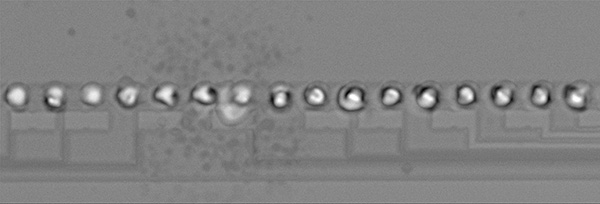
Figure 1. A gate that is too wide vertically puts too much information into a single acoustic image.
FIGURE 2 uses a much narrower gate to image the same flip chip. This gate is set at the upper range of the depth of interest. The top of the gate is in the silicon, and the bond sites are just becoming visible at this depth. Their material interfaces make all the bond sites visible, but one of the bonds (arrow) is very bright, suggesting cratering in the silicon above the bump.
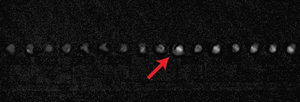
Figure 2. A narrower gate suggests that above one bump (arrow) there is cratering in the silicon.
Figure 2 was made using polygate mode, which allows multiple gates to be set before scanning begins. The value of a narrow gate is that it makes an image using only the echoes returned from a very limited time gate representing a very limited vertical range. If the operator of the acoustic micro imaging tool sets several gates, the data for each gate will be collected during the single scan of the transducer, and will be displayed as an acoustic image of that gate only.
How narrow can a gate be? The actual limit is a gate of 1ns thickness, meaning the distance that ultrasound travels is 1ns in a given material. The velocity of ultrasound in monocrystalline silicon is about 8433 meters per second. In one nanosecond, ultrasound will travel 8.433µm. Most materials have lower acoustic velocities. In practice, a handful of gates may suffice (although hundreds can be set if desired).
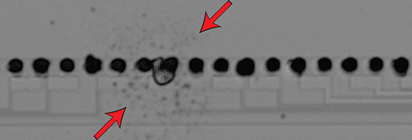
FIGURE 3 is the acoustic image from an equally narrow gate immediately beneath the gate shown in Figure 2. The data for this image were collected during the same scan as the data for Figure 2. The bright appearance of the bumps shows how extensive the laminar cracking is. In one spot (arrow) the cracking can be seen to extend outward under the passivation layer. The traces on the die are very faintly visible as pale features in this gate.
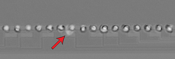
Figure 3. The next gate down suggests that cracking extends beneath the passivation layer.
FIGURES 4 and 5 show, in order, the next two gates in the sequence. The die traces become more visible in Figure 4 and are conspicuous in Figure 5. In both gates, the features seen as bright cracks in the gates above this depth are now very dark. When ultrasound strikes and is reflected from material interfaces as in Figures 4 and 5, it encounters and is reflected back by the cracks and other gap-type features above that depth – those in Figure 3, for example. The transducer thus receives no signal in these regions, and the corresponding pixels are black.
Figures 4 and 5. These samples are gated below the bumps, which now are displayed as dark acoustic shadows.
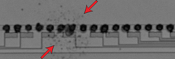
The arrows in the left half of Figures 4 and 5 indicate small dark spots (arrows). The spots are some type of contamination on the inner die surface.
Frequency domain imaging. The polygate mode described above is one of several modes that use time domain imaging. Frequency domain imaging (FDI) analyzes the ultrasonic frequency content rather than the amplitude of the echoes, and can be useful in bringing out subtle details in the acoustic image of a flip chip.
When a 100MHz transducer, for example, pulses ultrasound into a sample, the return echoes from a given interface may include a range of frequencies from about 50 to 150MHz. In time domain (amplitude mode) imaging, only the amplitude is used to produce the acoustic image.
When all of the gated A-scan echoes for each x-y coordinate of a sample are collected, they can be decomposed by means of a Fast Fourier Transform into individual sinusoids. FIGURE 6 is a simulation showing how a 100MHz echo can be decomposed into individual sinusoids. Three of the sinusoids that combine constructively or destructively to create the broadband time domain waveform are shown above it.
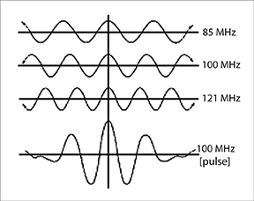
Figure 6. The time domain waveform (bottom) can be decomposed into the three individual sinusoids at the top to produce individual acoustic images.
What this means is a Fast Fourier Transform can decompose A-scans to yield a separate acoustic image for each sinusoid. There may be a dozen or more such images. Typically this method provides higher resolution.
In FIGURE 7 are a time domain (top) and a frequency domain image (bottom) of a flip chip having many features but no defects. One section of each image is enlarged to show contrast and resolution. In the time domain image, the amplitude determines the pixel color at each X-Y location, regardless of the frequency of the echo, which may range, in the case of a 400MHz transducer, from about 300 to 500MHz or more.
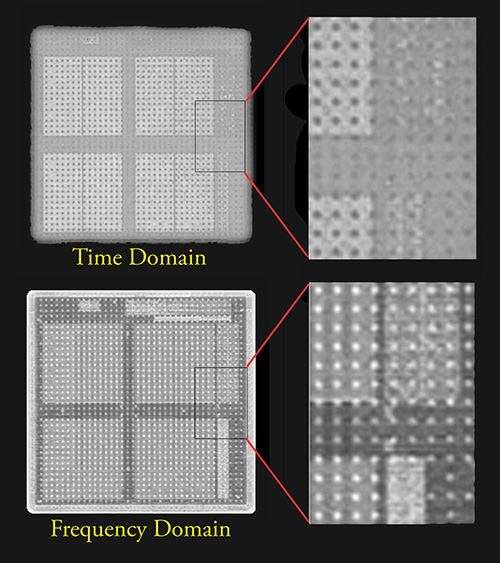
Figure 7. One of the frequency domain images (bottom) gives more detail and contrast than the time domain image (top).
The frequency domain image is one of several images made by transforming the A-scans. It has a higher resolution than the time domain image and demonstrates that, among the FDI images made of a flip chip, one or more will likely have superior resolution of fine details. Users of frequency domain imaging soon learn that, among the dozen or more FDI images of a flip chip, one or two images are likely to display the resolution that is needed to analyze a defect and solve a problem.
is a consultant to Sonoscan Inc. (sonoscan.com); tom100adams@comcast.net.


