

Current Issue
Rigid-Flex PCB Design for an Innovative Helmet-Mounted Display
Developing a wearable high-speed board with severe timing constraints.
The US Air Force engaged HoloEye Systems to create a prototype binocular holographic waveguide visor display (HWVD) attached to the helmet worn by a pilot of an Air Force jet. Advanced sensors throughout the aircraft generated key info that the pilot needed. This helmet-mounted display (HMD) presented a heads-up display of instrumentation and digital representations of important data. The helmet was the heart of the aircraft, enabling the pilot to take advantage of the whole system.
This cutting-edge technology significantly decreased the cost, volume and weight of traditional helmet-mounted displays, replacing bulky optics systems with thin, light-weight, see-through diffractive optics. The headset display was one of the first reported binocular HMDs in development using a liquid crystal and silicon (LCOS) microdisplay.
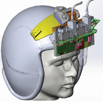
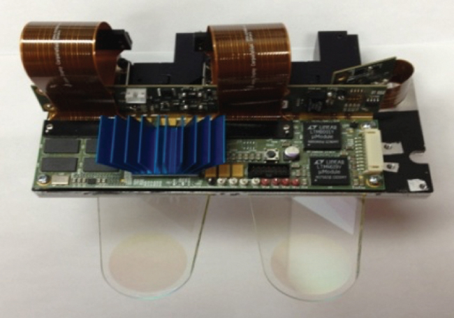
Figure 1. The stereo microdisplay controller was designed for a binocular holographic waveguide visor display to be worn by an Air Force pilot.
PCB requirements. The helmet-mounted display supported the PCB in its mechanical housing, and an HDMI cable fed into the video source. An optical cable connected to the display, which carried light to the headset’s LCOS microdisplay. The light illuminated the display and was projected onto waveguides that presented information to the pilot’s eyes.
The display’s physical requirements posed interesting challenges for the PCB. First, the system needed to be small enough to mount to the pilot’s helmet and allow for motion without causing discomfort. Second, to avoid pilot injury, it needed to immediately release all connections to the plane in the event the pilot needed to eject from the aircraft. Third, the boards needed to be flexible enough to wrap around the system’s optical components and accommodate connectors at different angles. Fourth, as a result of size constraints, the design could only break out traces on the eastern and western sides of the main FPGA component, instead of a north-south-east-west pattern.
The design used a Xilinx FPGA and a 64-bit wide DDR3 memory bus, where each of four components had a 16-bit wide data bus. One of the more challenging parts of the design was that the connection between the FPGA and memory required simulation at a very high speed, so the timing constraints were tight. Timing was matching to a few picoseconds on the flight times through the board. With such tight margins, it was important to consider the travel time of flight inside the packages as well as on the board. For these reasons, die-to-die time of flight was chosen, as opposed to just pin-to-pin time of flight.
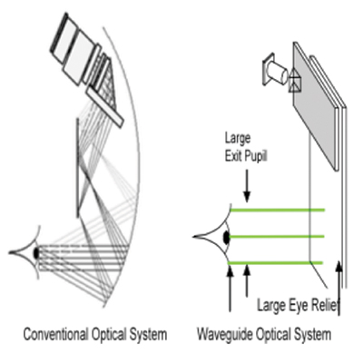
Figure 2. In the waveguide optical system, light was projected onto waveguides that presented information to the pilot’s eyes (image courtesy of BAE Systems).
Xilinx provided useful information about time of flight inside the package, as did the IBIS models of the Micro memory modules. The package for the memory component was significantly smaller than the Xilinx FPGA, and the Xilinx time of flight information was crucial. We were able to tweak out the differences in the memory parts after layout was completed.
There were two parts to the simulation. The first was to ensure signal integrity; considerations for impedance matching would ensure no impedance discontinuities would cause signal integrity issues. While the signal speeds were high, they were not high enough for loss to be a significant concern, given the trace lengths involved.
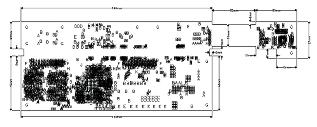
Figure 3. The PCB design used a Xilinx FPGA and a 64-bit wide DDR3 memory bus.
The second part of the simulation was an interesting task: to ensure that the design met the timing requirements of the DDR3 by considering time and length match.
The trace length between the memories and FPGA varied between 1.5" to several inches in length. The address and control signals traveled to all four memory components, whereas the data and DQS traveled simply as a point to point for each lane. The clock path for the address and control signals needed to be the longest path because the DDR3’s write timing system could not manage a situation in which the clock path was shorter than the data path. This caused difficulty because the clock was coming from a certain part of the FPGA, while the data were coming from a part of the FPGA that was potentially farther away. It was a challenge to maintain delays so that the write timing in the DDR3 would work.
One of the DDR3 requirements was that the address and control data would be presented in a fly-by mode, connecting between the controller and all four memory ICs. Signal integrity needed to be excellent at the first and last memory IC, and the terminations needed to be correct. In addition to this, for the first and second memory IC, earlier along the path, the data sometimes came from a part of the FPGA, which made the data path quite long. To adhere to the timing constraint that required the clock path to be longer than the data and DQS lines, one had to add length to the clock. This, of course, conflicted with space requirements.
To ensure timings matched, basic routing was performed first and then matched the lengths. It was decided which layers would be used for each of the signals and groups travelled together; for example, each data lane was placed on the same layer. An effort was made to minimize the number of vias and other features needed to reach the end path.
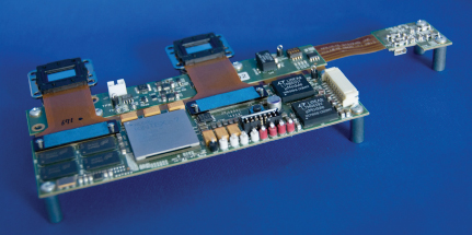
Figure 4. The main board and first flex section of the final stereo microdisplay controller were 140 x 65mm. The flex extension on the right-hand side was 62 x 27mm.
The challenge came when it was time to match segments. This was difficult due to the lack of space. A simple point-to-point match for the address and control lanes wouldn’t suffice. Instead, we matched every segment: between the controller and the first IC, first IC to the second IC, and so on. Luckily, because the ICs were a specific distance apart, it was essentially a point-to-point match, and the trace lengths were similar. The biggest challenge was matching the segment from the FPGA to the first memory IC, where we were constrained by the positions of the signals on the FPGA, which could be quite diverse in their distances from the memory IC. The longest path defined how long the trace needed to be, and in some cases we needed to increase the trace by a large fraction of an inch to accommodate this. To add so much length, trombones or accordions were needed, which took up space on the board.
The FPGA had some flexibility with respect to which pins could be used for which purposes. However, as speed increased, it posed constraints because specific groups of pins for specific lanes of data were needed. There were also a number of pins designed specifically to be used with DDR3. The biggest problem came with the address and control lanes, all traveling in large groups on the same layers of the board. Ingenuity was certainly needed to include all the trombones and accordions required to match lengths in the limited space.
Controlled impedance requirements. The HDMI video input had several different requirements for controlled impedance. The length of the trace used was very small, and the signals were relatively slow compared to DDR, so trace length wasn’t a problem. However, the HDMI required 100Ω differential pairs, while the memory ran at 80Ω. Therefore, it was an interesting challenge to ensure controlled impedance, and it was difficult to come up with a board stackup that would leave adequate space for 80Ω, as well as 100Ω, without becoming too thin and difficult to manufacture.
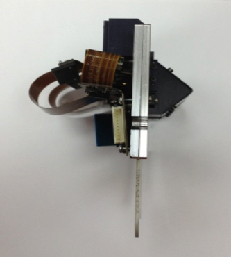
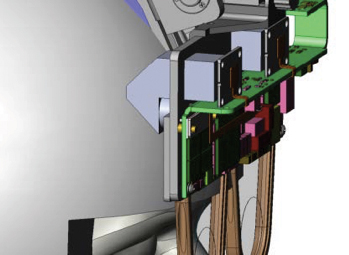
Figures 5, 6 and 7. The PCB wrapped around the optical components of the HWVD system, accommodating various connector angles.
The BGA packages for the FPGA and HDMI controller posed trace breakout issues. Although the FPGA wasn’t a particularly large or dense part, because of the board’s small size, traces could only break out on the east and west sides instead of the traditional north-south-east-west pattern. Similarly, the HDMI controller was a very fine-pitch BGA; it didn’t have very many pins, but it was a 0.5mm pitch BGA, so breaking out in a traditional pattern would be difficult.
High-density interconnect techniques and blind and buried vias were employed to break out traces from the FPGA and HDMI controller. The HDMI controller pattern also used via-in-pads. Sierra Circuits’ HDI Stackup Planner tool was used to simulate board stackup. It was useful to perform some “what-if” scenarios and see how the stackup could potentially come out, without explaining or providing too much information about my project. We went through a few iterations on that, with a few different kinds of materials, looking at the impedance planning.
At first, FR-4 material was under consideration, but after some scenarios using the Sierra Circuits Impedance Calculator, we decided to go with a material that had a lower dielectric constant, achieving signal integrity, low loss, and desirable line-space ratio for impedance controlled traces. Having a lot of this information already available and being able to play with it and say, ‘What if I do this? What if I do that?’ and actually having an estimate of how those changes would affect the producibility and the cost of the board was really useful.
Using HDI reduced the number of layers needed in the board overall, and after balancing the cost with the advantages of HDI technology, it was decided this was the right direction.
The rigid-flex solution. As the design moved forward and it became clear that space was a concern, it was decided to connect the rigid boards with a flex ribbon to avoid using standard physical connectors that required more space.
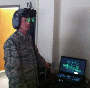
Figure 8. A team member demonstrates the working prototype helmet-mounted display.
There were three rigid sections in the final design: 1) A main section with the FPGA, DDR3 ICs, and power supply units; 2) a second section with slower, analog-type components and more power supplies; 3) a third section that featured a very small HDMI receiver with multiple possible orientations to accommodate the incoming input cable. This third satellite board took the high-speed HDMI and converted it to a slow-speed pixel array with a wide parallel bus, which connected to the FPGA for processing via the flex sections.
The final board stackup was 10 layers. The rigid boards used eight layers and carried all the impedance-controlled and high-speed traces. The other two layers were the flex signal layer, which was also used as the VCC layer in the main rigid part of the board. There was some collaboration between layers of the rigid and flex segments, but for the most part these were treated independently.
Anything that required impedance control was managed entirely within one of the rigid structures. Breaking it down into those sections allowed us to avoid any need for impedance control on the flex, which was a big win insofar as cost goes.
Rigid-flex permitted the board to fit into the small housing on the helmet-mounted display system. The flex ribbon could bend a number of ways, accommodate different angles, and be rolled up and fully consumed within the volume of the container, providing options on how the boards would enter into the system and wrap around the optical components.
Results. The team delivered the rigid-flex board to the Air Force in a binocular visor display prototype that met all requirements, on time. In all, 10 PCBs were designed, then fabricated and assembled with Sierra Circuits. The design performed well and balanced the right features, while keeping cost and manufacturability in mind. The board was one of the first reported developments of a binocular holographic waveguide aviation helmet-mounted display using LCOS.
is founder and principal engineer of GlyphLogic Consulting, a contract electrical engineering and PCB design service firm (glyphlogic.com).


Press Releases
- AIM Solder Promotes Timothy O’Neill to Vice President of Technology
- AIM Solder Hires Francisco Rodriguez as Regional Sales Manager for Northeast Mexico
- The Test Connection, Inc. Adds Creative Electron Prime TruVision™ X-ray and CT System for Deeper Failure Analysis
- Kurtz Ersa Goes Semiconductor: Expanding Competence in Microelectronics & Advanced Packaging