

Current Issue
Depaneling of Circuit Boards
A review of the impacts various methods have on the final product.
Several methods are practiced for depaneling printed circuit boards. They include:
- Punching/die cutting. This method requires a different die for each new circuit board, which is not a practical solution for small production runs. The action can be either a shearing or crushing method, but either can leave the board edges somewhat deformed. To minimize damage care must be taken to maintain sharp die edges.
- V-scoring. Typically the panel is scored on both sides to a depth of about 30% of the board thickness. After assembly the boards can be manually broken out of the panel. This puts bending strain on the boards that can be damaging to some of the components, especially those close to the board edge.
- Wheel cutting/pizza cutter. An alternate method to manually breaking the web after V-scoring is to use a “pizza cutter” to cut the remaining web. This requires careful alignment between the V-score and the cutter wheels. It also induces stresses in the board which may affect some components.
- Sawing. Typically machines that are used to saw boards out of a panel use a single rotating saw blade that cuts the panel from either the top or the bottom.
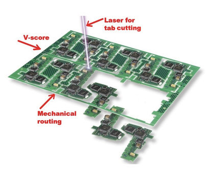
Figure 1. Combining various singulation methods in the same panel.
Each of these methods is limited to straight line operations, thus only for rectangular boards, and each of them to some degree crushes and/or cuts the board edge. Other methods are more expansive and include the following:
- Water jet. Some say this technology can be done; however, the authors have found no actual users of it. Cutting is performed with a high-speed stream of slurry, which is water with an abrasive. We expect it will require careful cleaning after the fact to remove the abrasive portion of the slurry.
- Routing (+nibbling). Most of the time boards are partially routed prior to assembly. The remaining attaching points are drilled with a small drill size, making it easier to break the boards out of the panel after assembly, leaving the so-called mouse bites. A disadvantage can be a significant loss of panel area to the routing space, as the kerf width typically takes up to 1.5 to 3mm (1/16 to 1/8") plus some additional space for inaccuracies. This means a significant amount of panel space will be needed for the routed traces.
- Laser routing. Laser routing provides a space advantage, as the kerf width is only a few micrometers. For example, the small boards in FIGURE 2 were initially laid out in anticipation that the panel would be routed. In this manner the panel yielded 124 boards. After designing the layout for laser depaneling, the number of boards per panel increased to 368. So for every 368 boards needed, only one panel has to be produced rather than three.
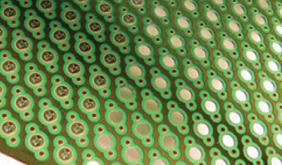
Figure 2. Example for a panel with very small circuits.
Routing can also reduce panel stiffness to the point that a pallet may be required for support during the earlier steps in the assembly process. But unlike the previous methods, routing is not limited to cutting straight line paths only.
Most of these methods exert some degree of mechanical stress on the board edges, which can lead to delamination or cause space to develop around the glass fibers. This can lead to moisture ingress, which in turn can reduce the long-term reliability of the circuitry.
Additionally, when finishing placement of components on the board and after soldering, the final connections between the boards and panel have to be removed. Often this is accomplished by breaking these final bridges, causing some mechanical and bending stress on the boards. Again, such bending stress can be damaging to components placed close to areas that need to be broken in order to remove the board from the panel. It is therefore imperative to take the production methods into account during board layout and for panelization so that certain parts and traces are not placed in areas known to be subject to stress when depaneling.
Room is also required to permit the precision (or lack thereof) with which the tool path can be placed and to take into account any non-precision in the board pattern.
Laser cutting. The most recently added tool to delaminate flex and rigid boards is a laser. In the SMT industry several types of lasers are being employed. CO2 lasers (~10µm wavelength) can provide very high power levels and cut through thick steel sheets and also through circuit boards. Neodymium:Yag lasers and fiber lasers (~1µm wavelength) typically provide lower power levels at smaller beam sizes. Both these laser types produce infrared light and could be called “hot” lasers as they burn or melt the material being cut. (As an aside, these are the laser types, especially the Nd:Yag lasers, typically used to produce stainless steel stencils for solder paste printing.)
UV lasers (typical wavelength ~355nm), on the other hand, are used to ablate the material. A localized short pulse of high energy enters the top layer of the material being processed and essentially vaporizes and removes this top layer explosively, turning it to dust (FIGURE 3).
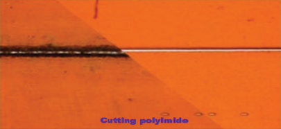
Figure 3. “Hot” laser on the left, “cold” UV laser on the right.
The choice of a 355nm laser is based on the compromise between performance and cost. In order for ablation to occur, the laser light has to be absorbed by the materials to be cut. In the circuit board industry these are mainly FR-4, glass fibers and copper. When looking at the absorption rates for these materials (FIGURE 4), the shorter wavelength lasers are the most appropriate ones for the ablation process. However, the laser cost increases very rapidly for models with wavelengths shorter than 355nm.
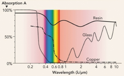
Figure 4. Energy absorption vs. wavelength.
The laser beam has a tapered shape, as it is focused from a relatively wide beam to an extremely narrow beam and then continuous in a reverse taper to widen again. This small area where the beam is at its most narrow is called the throat. The optimal ablation occurs when the energy density applied to the material is maximized, which occurs when the throat of the beam is just inside the material being cut. By repeatedly going over the same cutting track, thin layers of the material will be removed until the beam has cut all the way through.
In thicker material it may be necessary to adjust the focus of the beam, as the ablation occurs deeper into the kerf being cut into the material. The ablation process causes some heating of the material but can be optimized to leave no burned or carbonized residue. Because cutting is done gradually, heating is minimized.
The earliest versions of UV laser systems had enough power to depanel flex circuit panels. Present machines have more power and can also be used to depanel circuit boards up to 1.6mm (63 mils) in thickness.
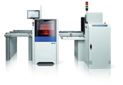
Figure 5. Example of a laser depaneling system in an inline setting for automatic load and unload.
Temperature. The temperature rise in the material being cut depends on the beam power, beam speed, focus, laser pulse rate and repetition rate. The repetition rate (how quickly the beam returns to the same location) is determined by the path length, beam speed and whether a pause is added between passes.
A knowledgeable and experienced system operator will be able to select the optimum combination of settings to ensure a clean cut free of burn marks. There is no straightforward formula to determine machine settings; they are influenced by material type, thickness and condition. Depending on the board and its application, the operator can choose fast depaneling by permitting some discoloring or even some carbonization, versus a somewhat slower but completely “clean” cut.
Careful testing has shown that under most conditions the temperature rise within 1.5mm from the cutting path is less than 100˚C, way below what a PCB experiences during soldering (FIGURE 6).
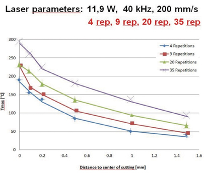
Figure 6. Heating along cutting path.
Expelled material. In the laser used for these tests, an airflow goes across the panel being cut and removes most of the expelled dust into an exhaust and filtration system (FIGURE 7).
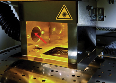
Figure 7. Removal of dust.
To test the impact of any remaining expelled material, a slot was cut in a four-up pattern on FR-4 material with a thickness of 800µm (31.5 mils) (FIGURE 8). Only few particles remained and consisted of powdery epoxy and glass particles. Their size ranged from an average of 10µm to a high of 20µm, and some may have consisted of burned or carbonized material. Their size and number were extremely small, and no conduction was expected between traces and components on the board. If so desired, a simple cleaning process could be added to remove any remaining particles. Such a process could consist of the use of any kind of wiping with a smooth dry or wet tissue, using compressed air or brushes. One could also use any kind of cleaning liquids or cleaning baths with or without ultrasound, but normally would avoid any kind of additional cleaning process, especially an expensive one.
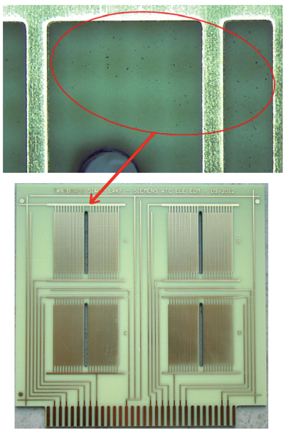
Figure 8. Surface after laser cutting.
Surface resistance. After cutting a path in these test boards (Figure 7, slot in the middle of the test pattern), the boards were subjected to a climate test (40˚C, RH=93%, no condensation) for 170 hr., and the SIR values exceeded 10E11 Ohm, indicating no conductive material is
present (FIGURE 9).
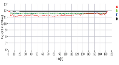
Figure 9. Surface resistance.
Cutting path location. The laser beam typically uses a galvanometer scanner (or galvo scanner) to trace the cutting path in the material over a small area, 50x50mm (2x2"). Using such a scanner permits the beam to be moved at a very high speed along the cutting path, in the range of approx. 100 to 1000mm/sec. This ensures the beam is in the same location only a very short time, which minimizes local heating.
A pattern recognition system is employed, which can use fiducials or any other panel or board feature to precisely find the location where the cut has to be placed. High precision x and y movement systems are used for large movements in combination with a galvo scanner for local movements.
In these types of machines, the cutting tool is the laser beam, and it has a diameter of approximately 20µm. This means the kerf cut by the laser is about 20µm wide, and the laser system can locate that cut within 25µm with respect to either panel or board fiducials or any other board feature. The boards can therefore be placed very close together in a panel. For a panel with many small circuit boards, additional boards can therefore be placed, leading to cost savings.
As the laser beam can be freely and rapidly moved in both the x and y directions, cutting out irregularly shaped boards is simple. This contrasts with some of the other described methods, which can be limited to straight line cuts. This becomes advantageous with flex boards, which are often very irregularly shaped and in some instances require extremely precise cuts, for example when conductors are close together or when ZIF connectors need to be cut out (FIGURE 10). These connectors require precise cuts on both ends of the connector fingers, while the fingers are perfectly centered between the two cuts.
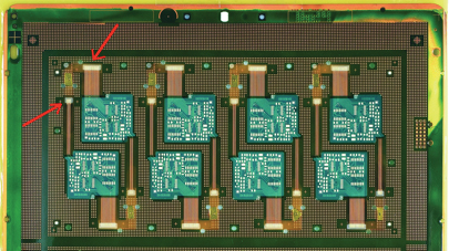
Figure 10. Flex circuit with ZIF connectors.
A potential problem to consider is the precision of the board images on the panel. The authors have not yet found an industry standard indicating an expectation for board image precision. The closest they have come is “as required by drawing.” This problem can be overcome by adding more than three panel fiducials and dividing the cutting operation into smaller sections with their own area fiducials. FIGURE 11 shows in a sample board cut out in Figure 2 that the cutline can be placed precisely and closely around the board, in this case, next to the outside of the copper edge ring.
Figure 11. Singulated board from Figure 2, slightly oblique.
Even when ignoring this potential problem, the minimum space between boards on the panel can be as little as the cutting kerf plus 10 to 30µm, depending on the thickness of the panel plus the system accuracy of 25µm.
Within the area covered by the galvo scanner, the beam comes straight down in the middle. Even though a large collimating lens is used, toward the edges of the area the beam has a slight angle. This means that depending on the height of the components near the cutting path, some shadowing might occur. As this is completely predictable, the distance some components need to stay removed from the cutting path can be calculated. Alternatively, the scan area can be reduced to side step this problem.
Stress. As there is no mechanical contact with the panel during cutting, in some instances all of the depaneling can be performed after assembly and soldering (Figure 11). This means the boards become completely separated from the panel in this last process step, and there is no need for any bending or pulling on the board. Therefore, no stress is exerted on the board, and components near the edge of the board are not subject to damage.
In our tests stress measurements were performed. During mechanical depaneling a significant snap was observed (FIGURES 12 and 13). This also means that during earlier process steps, such as paste printing and component placement, the panel can maintain its full rigidity and no pallets are required.
Figure 12. Stress during laser depaneling, not measurable.
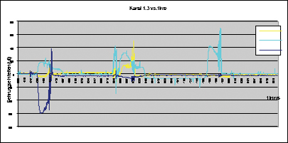
Figure 13. Stress during mechanical depaneling.
A common production method is to pre-route the panel before assembly (mechanical routing, using a ~2 to 3mm routing tool). Rigidity is then determined by the size and quantity of the breakout tabs. The final depaneling step will generate even less debris, and by using this method laser cutting time is reduced.
After many tests it has become clear the sidewall of the cut path can be very clean and smooth, regardless of the layers in the FR-4 boards or polyimide flex circuits. If the need for a clean cut is not very high, as in tab cutting of a pre-routed board, the cutting speed can be increased, resulting in some discoloration (FIGURE 14).
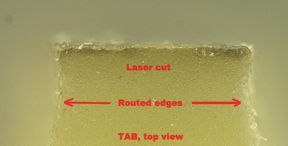
Figure 14. Laser cut tab.
When cutting through epoxy and glass fibers, there are no protruding fibers or rough edges, nor are there gaps or delamination that would permit moisture ingress over time (FIGURE 15). Polyimide, as used in flex circuits, cuts well and permits for extremely clean cuts, as seen in Figure 3 and in the electron microscope picture in FIGURE 16.
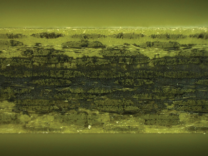
Figure 15. Laser cut edge.
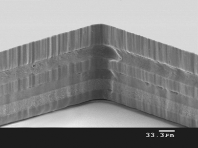
Figure 16. Electron microscope image of cutting path in multilayer polyimide.
As noted, it is necessary to keep the material to be cut by the laser as flat as possible for optimum cutting. In certain instances, as in cutting flex circuits, it can be as easy as placing the flex on a downdraft honeycomb or an open cell foam plastic sheet. For circuit boards it may be more difficult, especially for boards with components on both sides. In those instances it still may be desirable to prepare a fixture that can accommodate odd shapes and components.
Conclusions
Laser depaneling can be performed with very high precision. This makes it extremely useful in situations where parts of the board outline demand close tolerances. It also becomes appropriate when very small boards are involved. Because the cutting path is very narrow and can be located very precisely, individual boards can be placed closely together on the panel.
The low thermal effects mean that even though a laser is involved, minimal temperature increases occur, and therefore essentially no carbonization results.
Depaneling occurs without physical contact with the panel and without bending or pressing; therefore there is less chance of component failures or future reliability issues.
Finally, the location of the cutting path is software-controlled, which means changes in boards can be handled quickly.
Acknowledgments
Images provided by LPKF USA and LPKF Laser & Electronics AG, Garbsen, Germany.
Ed.: This article was originally published in the Proceedings of the 20th Pan Pacific Microelectronics Symposium in February 2015 and is reprinted here with permission of the authors.
Bibliography
- Ahne Oosterhof, Mark Hueske and Dr. Dieter Meier, “Laser Ablation – Cutting Systems for the Electronics Industry,” Industrial Laser Solutions, June 2007.
- Shane Stafford, “Flex Circuit Depaneling: How UV Lasers Meet Today’s Trends,” Industrial Laser Solutions, September 2012.
- Dr. Dieter J. Meier and Stephan H. Schmidt, “PCB Laser Technology for Rigid and Flex HDI – Via Formation, Structuring, Routing,” IPC Printed Circuits Expo, March 2002.
- Maria Fontanazza, “Failure Isn’t an Option,” Medical Device and Diagnostics Industry, March 2010.
- Manfred Zäske, “Laser Cutting of Printed Circuit Boards: Evaluation of Possible Corrosive Effects of Residuals Using SIR Test and Optical Inspection,” CT RTC ELE EOM-DE, June 2013.
is a consultant with Eastwood Consulting and is project manager of Microline UV systems at LPKF (lpkfusa.com/depaneling.com); ahne@oosterhof.com.


