Current Issue
Extreme Long-Term PCB Surface Finish Solderability Assessment
Could a mix of finishes hold up after 20 years in storage?
The 1995/96 testing included solderability testing in accordance with IPC J-STD-002, surface finish oxidation assessment using Sequential Electrochemical Analysis (SERA), and ball bond/wedge bond wirebondability testing in accordance with the MIL-STD-883D, Method 2011.7, test condition C procedures. Testing revealed ENIPIG and the electroless palladium surface finish combinations achieved the desired solderability, shelf life and wirebondability goals. The ENIPIG surface finish was substituted for the dual-gold plating finish configuration to reduce costs and improve overall product integrity.
Table 1. Printed Circuit Board Surface Finishes Tested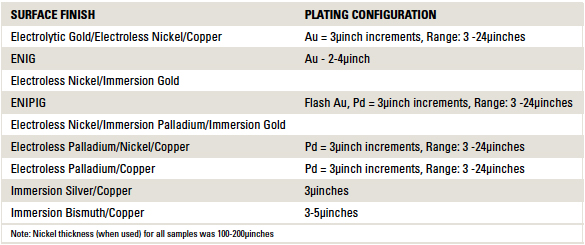
Spare test specimens with the investigation surface finishes were produced for the study but were not utilized during testing. These specimens were placed in non-sealed polyethylene bags, stored in a 21ºC/30%-65% RH environment and promptly forgotten. The specimens were rediscovered in 2015 after accumulating 20 years of total storage time, thereby providing an opportunity to investigate extreme long-term solderability of a well-characterized set of surface finishes.
Test specimen. The test specimen was a bismaleimidc-triazine (BT) laminate, 0.040" thick with 0.5 oz. copper outer layers sheared into 3" x 3" squares. These 3" x 3" substrates were electroplated with approximately 0.001" of copper prior to the application of each specific test surface finish. The test substrates that contained a nickel layer had approximately 0.0001" to 0.0002" of electroless nickel plating deposited. The 3" x 3" test substrates were diamond cut into six sections approximately 0.5" wide after plating for use in the 1995-96 evaluation. A total of three to five spare specimens that were 20-years-old of each surface finish were available for the new solderability investigation.
Test plan. A sample from each of the surface finishes and thicknesses was initially tested using a Metronelec ST88 wetting balance, following the protocol detailed in IPC J-STD-003C-WAM1. These samples were tested using eutectic SnPb solder and using the prescribed test flux #1. The test temperature was 235°C with a dwell time of 10 sec. in the solder pot. Only two sample groups failed to produce positive wetting forces: the single thickness sample of immersion bismuth and the 3µin palladium over copper sample. Based on these initial screening results, additional samples were cut at random from the sample strips and were tested using the same test protocols. A number of selected samples were assessed using focused ion beam (FIB) microscopy. An FEI Quanta 200-3D dual beam system with a gallium target ablation source and a maximum ablation rate of 0.5µm/min. was used. A layer of platinum was vapor-deposited on the test samples prior to FIB analysis to prevent extraneous ablation damage. Sample assessment was also conducted using a Fischer Technologies XDV-SDD x-ray fluorescence (XRF) system.
Results
Immersion bismuth. Upon visual examination, the immersion bismuth surface finish test coupons appeared heavily oxidized. Wetting balance testing results showed no positive wetting forces were produced, further indicating the bismuth surface finish had diffused into the underlying copper. FIGURE 1 illustrates immersion bismuth wetting balance results.
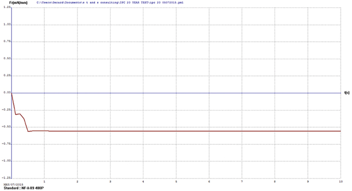
Figure 1. Immersion bismuth wetting balance results.
Immersion silver. The immersion silver surface finish test coupons exhibited some oxidation upon visual examination. Wetting balance testing results showed slow initial wetting times with final positive wetting forces (FIGURE 2). These wetting balance values indicate degradation of the immersion silver surface but no negative impact of diffusion issues as were observed with the immersion bismuth surface finish.
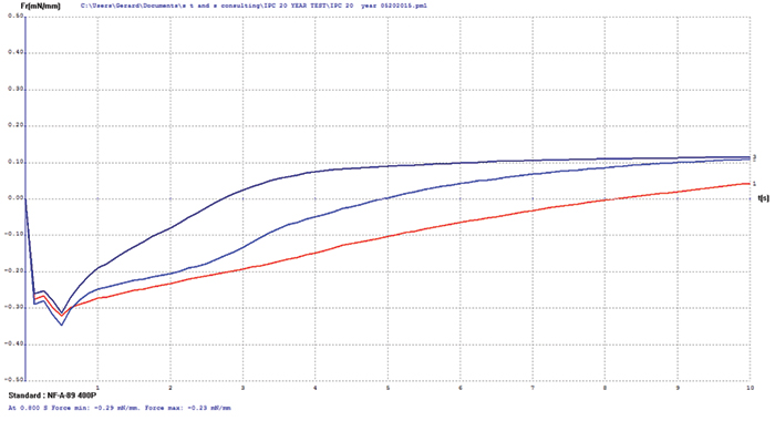
Figure 2. Immersion silver test coupon wetting balance results (three individual test coupons).
Since current immersion silver surface finishes are typically eight to 16µin thick, it was speculated the original 3µin layer was consumed by oxidation and/or diffusion after 20 years of storage. XRF assessment measured 1.2µin of immersion silver, while FIB assessment measured the immersion silver deposit closer to 2.4µin in thickness (FIGURE 3).
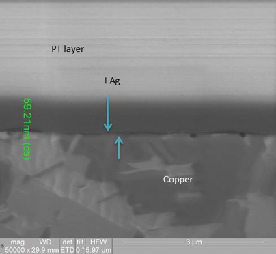
Figure 3. FIB image of immersion silver deposit (50,000X magnification).
Electroless palladium/copper. The electroless palladium surface finish test coupons covered a palladium thickness range of 3 to 21µin, and some coupon oxidation was evident by visual examination prior to testing. Wetting balance testing results (FIGURE 4) merge multiple tests for electroless palladium with increasing palladium thickness. The thinnest sample, nominally 3µin, was the only group that failed to produce positive wetting forces. The initial wetting times and final forces for the remaining sample groups are very consistent with palladium thickness overall, indicating no apparent negative impact on the protection of the underlying copper for palladium finishes in excess of 3µin.
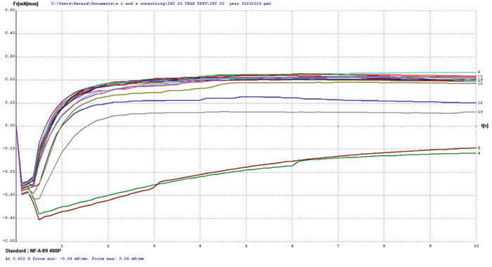
Figure 4. Electroless palladium test coupon wetting balance results (test coupons covering 3-21µin range).
FIB and XRF assessment were conducted to characterize changes in the electroless palladium layer after 20 years of storage. XRF assessment found no evidence of electroless palladium, but FIB assessment measured the electroless palladium deposit at 0-0.3µin in thickness (FIGURE 5) for the 3µin electroless palladium sample. However, for the 6µin electroless palladium sample, the XRF measurement was 5.6µin, and the FIB measurement was 4 to 6µin (FIGURE 6).
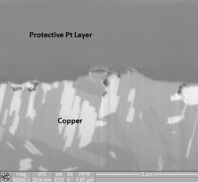
Figure 5. FIB image of nominal 3µin electroless palladium deposit (50,000X magnification).
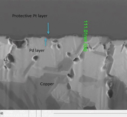
Figure 6. FIB image of nominal 6µin electroless palladium deposit (50,000X magnification).
Electroless nickel/immersion gold (ENIG). FIGURE 7 shows wetting balance test data for the ENIG surface finish. Wetting times are somewhat slow and the rates of rise low, which is characteristic of ENIG with some age or stress on the deposit. The porous immersion gold deposit offers good protection to the underlying nickel but not enough to prevent the occurrence of some oxidation. However, the final wetting forces are excellent and meet the requirements of the soon-to-be-released IPC-4552A specification. Increasing flux activity would have a dramatic impact on wetting times and rate of rise but little on the final wetting forces.
FIB and XRF assessment were conducted to characterize the changes in the ENIG plating after 20 years of storage. XRF assessment measured the immersion gold deposit at 4.9µin and the electroless nickel at 406µin. FIB assessment measured the immersion gold deposit at 2.4µin and the electroless nickel at 400µin (FIGURE 8).
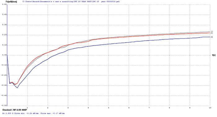
Figure 7. ENIG test coupon wetting balance results (three individual test coupons).
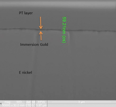
Figure 8. FIB image of ENIG deposit (50,000X magnification).
Electroless nickel/electroless palladium. FIGURE 9 shows wetting balance test data for electroless nickel/electroless palladium. Overall this group exhibited excellent robustness, with the majority wetting in less than 1 sec. The rates of rise are good, which indicated the presence of only a minor oxide layer that was easily reduced by the rather inactive test flux #1. The spread in the final wetting forces is relatively small, with final forces somewhat lower than ENIPIG surface finish, but excellent overall given the age of the samples.
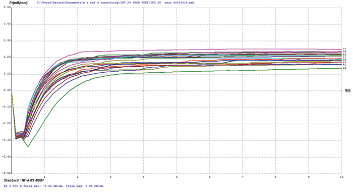
Figure 9. Electroless nickel/electroless palladium test coupon wetting balance results.
XRF assessment measured the electroless palladium at 5.11µin and the electroless nickel at 180µin, with the FIB assessment measuring the electroless palladium deposit at 2.6µin and the electroless nickel at 188µin (FIGURE 10) for the 3µin electroless palladium sample. For the 6µin electroless palladium sample, the XRF measurement was 5.95µin for the electroless palladium and 298µin for the electroless nickel, with the FIB measurement at 2.1µin for the electroless palladium and 312µin for the electroless nickel (FIGURE 11).
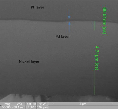
Figure 10. FIB Image of 3µin electroless nickel/electroless palladium deposit (50,000X magnification).
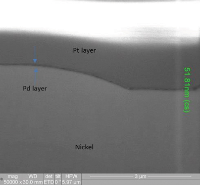
Figure 11. FIB image of 6µin electroless nickel/electroless palladium deposit (50,000X magnification).
Electroless nickel/immersion palladium/immersion gold (ENIPIG). FIGURE 12 shows wetting balance test results for the ENIPIG surface finish. Use of immersion gold over the immersion palladium dramatically improved the robustness of the deposit. Wetting times were excellent at under 0.5 sec, even after 20 years of storage. The rates of rise are also excellent to a final wetting force that meets the current requirements of IPC-4556. FIB and XRF assessment were not conducted on the ENIPIG surface finish due to sample quantity constraints.
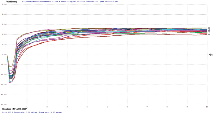
Figure 12. ENIPIG test coupon wetting balance results (3-24µin coupons).
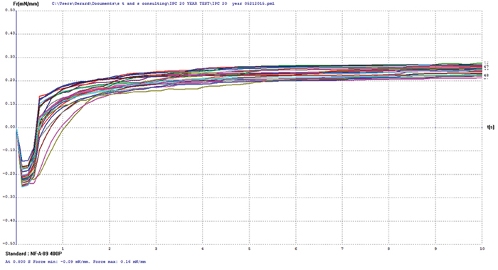
Figure 13. Electroless nickel/electrolytic gold test coupon wetting balance results.
Copper/electroless nickel/electrolytic gold. FIGURE 14 shows wetting balance test results for the electroless nickel/electrolytic gold surface finish. The thinnest nominal gold deposit was 5µin. The consistency of the group is excellent, with the majority producing positive wetting forces in less than 1 sec. The rates of rise to the final wetting forces are similarly excellent, indicating the gold layer has protected the underlying nickel from passivation.
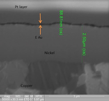
Figure 14. FIB image of electroless nickel/electrolytic gold deposit (50,000X magnification).
XRF assessment measured 5.8µin of electrolytic gold and 92µin of electroless nickel. The FIB assessment measured 3.6µin of electrolytic gold and 100µin of electroless nickel (Figure 9).
Discussion
Printed circuit board surface finishes have evolved during the past 20 years, so the surface finishes in the study are not “apples to apples” with ones used today. Modern board surface finishes are clearly better in terms of consistency/reproducibility, which makes positive solderability test results of these 20-year-old surface finishes reassuring. The following discussion points can be drawn from the data:
- The primary driving mechanisms for loss of solderability – oxidation and diffusion – were confirmed in the test results. FIB and XRF assessment revealed the 3µin surface finish coupons were significantly degraded after 20 years of storage. The ability of different plating metallurgies and plating combinations to reduce surface finish oxidation and diffusion mechanisms was realized on the surface finishes tested.
- The immersion silver surface finish did surprising well despite its thinness. IPC-4553 requires a significantly thicker plating to avoid the impact of storage and solder processing. The study testing results reaffirm the validity of the specification position/data covering the current immersion silver plating thickness requirements.
- The importance of having a nickel plating barrier to reduce the impact of diffusion was demonstrated. Nickel plating prevented the adverse effects of the copper diffusion on a number of the surface finishes.
- The importance of having immersion gold plating over the palladium plating to reduce the impact of surface oxidation/interface reactions was demonstrated. The immersion gold plating reduced the oxidation of the underlying surface finish and improved the solderability results.
- A storage condition of 21ºC/30%-65% RH in non-sealed polyethylene bags is not a particularly harsh environment, but is representative of many board storage environments used in industry today. The study test results are not representative of more severe board storage environments, but the results do demonstrate that properly processed, controlled surface finishes can have extremely long storage lives under specific conditions.
Conclusion
The study test results show that a variety of printed circuit board finishes subjected to a storage condition of 21ºC/30%-65% RH in non-sealed polyethylene bags maintained acceptable industry solderability test results after 20 years.
References
1. D. Hillman, P. Bratin, M. Pavlov, “Wirebondability and Solderability of Various Metallic Finishes for Use in Printed Circuit Assembly,” SMI Conference Proceedings, 1996.
Acknowledgments
The authors would like to thank Hank Lajoie and Lisa Gamza of MacDermid Enthone Electronic Solutions for outstanding focused ion beam (FIB) microscopy/XRF analysis, and Ross Wilcoxon, Rockwell Collins, for his scathing review of the manuscript.
Ed.: This article was first published in the SMTA International Conference on Soldering and Reliability Proceedings and is reprinted here with author permission.
is president of Solderability Testing and Solutions (standsgroup.com) and is principal materials and process engineer at Rockwell Collins (rockwellcollins.com); david.hillman@rockwellcollins.com.
Press Releases
- Saki to Highlight Advanced Inspection Innovation at 39th Nepcon Japan
- ViTrox Welcomes Gemaddis as a New Sales Channel Partner in France
- NCMS Releases White Paper: “Artificial Intelligence to Improve Supply Chain Resilience Throughout American Manufacturing”
- E-tronix Expands Team with Strategic Hires to Strengthen Technical Solutions Support in 2025


