Understanding 3D AOI, What It Is, and What It Isn’t
Do the limits of 2D cameras cast a shadow on their future? by Axel Lindloff
3D inspection has become a buzzword in the industry, but neither the meaning nor the definition of three-dimensional inspection has been standardized. What is behind the buzzword, and what are the different approaches currently offered to electronics manufacturers?
A number of systems and vendors have successfully used 3D measurement for years, but predominantly in the form of solder paste inspection (SPI) or, more correctly, solder paste measurement. It is necessary to differentiate between measurement and inspection, since 3D systems actually measure the solder paste volume deposited on the individual pads. Deploying different measurement technologies such as laser triangulation or phase shift profilometry achieves reasonably good results in performing 3D volumetric measurement, but the task is relatively simple: simply measuring bricks of dull, grey solder paste.
The success of 3D solder paste measurement during the past decade is proven through the process improvements that these systems have contributed to electronics manufacturing, particularly to the paste printing process. The adoption rate of 3D SPI systems in electronics manufacturing has grown from approximately 15% for all SMT lines a decade ago to market coverage of nearly 60% today.
Whether the same measurement technologies used for solder paste can be applied to solder joints depends on the technology. One proven technology in conducting real 3D measurements of solder joints is phase shift profilometry. The task of measuring curved and highly reflective solder joints is complex. The shiny surface and the multi-angled curvature of the solder joint complicate the ability for a laser to map all areas. Similarly, when applying light as the part of the measurement technology regardless of LED or flash, white or multi-colored, specula reflection has to be overcome as an obstacle to obtaining information from certain regions. Multiple directions of light projections must be used in order to compensate for this specula reflection. Too few light directions will not permit such compensation.
In the current debate, 2D AOI technology, which has been deployed for the past 25 years, can’t be overlooked. AOI was the only technology available to replace manual human inspection of assembled PCBs. That there are more than 25 AOI companies worldwide illustrates the need and importance of end-of-line or solder joint inspection in electronics manufacturing. These systems are now active on more than 90% of all SMT lines, and thus much more than that of SPI systems.
Since 2D systems deploy light from multiple angles onto the PCB, components and solder joints, all results for inspection depend on either contrast (e.g., location and polarity measurement) or location of reflection points (solder joint inspection). Figure 1 shows examples of chip resistors with different solder volumes under different light angles.
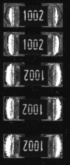
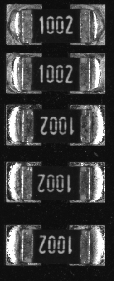
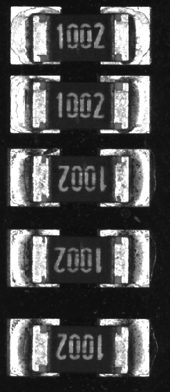
Figure 1. Chip resistors under (a) low angled light, (b) medium angled light and (c) top angled light.
Even when multiple camera or viewing angles are used, the results are still based on the availability of the applied light. Herein lies the problem; taller components will cast shadows on other components and solder joints. The different lighting conditions resulting from shadowing require the AOI programmer to modify thresholds on a component-by-component basis. As the same type of components on the same board have different thresholds applied, this leads to different defect detection capability and varying amounts of false fails.
Figure 2 shows a typical scenario whereby the same types of leads on the IC will require different settings due to the shadow from the Al-Cap.
Is 3D measurement applicable and really necessary for every aspect of the components and solder joints? Can certain attributes not be inspected in 2D, as they have been for many years?
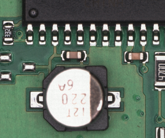
Figure 2. The tall capacitor casts a shadow on adjacent parts, requiring AOI setting modifications.
The advantages of 3D measurement lie in the word measurement. If you can measure the volume of each and every visible solder joint of every component, why would you just satisfy yourself with counting the bright pixels that the solder curvature is reflecting from an angled light source? Figure 3 shows a comparison of solder joints, measured in terms of their respective solder volumes.
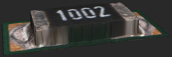
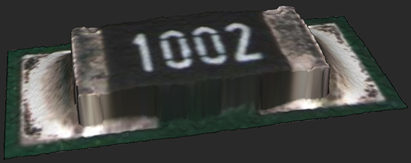
Figure 3. A chip resistor with (a) 15% solder volume and (b) 95% solder volume.
Why discriminate the edges of the component through different colors or grey scales, if the edge can be measured without the influence of component or PCB color in the third dimension? Figure 4 shows a typical scene of a chip resistor, which can be of varying color against the background of a PCB, which can also be of a different hue. Figure 5 shows the 3D image of the same component, where each pixel is measured for its height.
Figure 4. A resistor location shown in 2D.
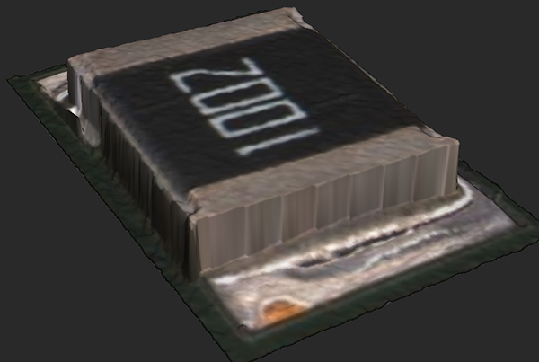
Figure 5. The same part in 3D.
Currently, AOI systems come with different levels of 3D coverage for components and solder joints. All 3D systems still offer 2D lighting and 2D inspection. It is for the AOI programmer or the QA department to decide to what extent they’d like to deploy new technology for quality assurance.
Contrary to common opinion, the polarity of components is typically a geometric feature rather than just a print. Those chamfers, dimples or corners can easily be measured in the third dimension, rather than relying on varying color and intensity of the print on the surface.
Should you measure certain aspects of the component in 3D, such as component location, and other attributes in traditional 2D? The solder joint is a three-dimensional structure as well. From a measurement perspective, we think applying the lower level 2D technology to the most critical feature on the PCB, the solder joint, doesn’t make sense. Instead, applying 3D measurement to as many aspects of the components and solder joints on a PCB is the best approach to improving the quality assurance of assembled PCBs, by utilizing true measurement technology with quantifiable measurement thresholds. For example, it is easy to understand that a lead is lifted for 170µm and hence is bad (out of range) if the applied threshold is 150µm. No more interpretation of this result is necessary, no image processing knowledge required and certainly no room for false calls or false accepts. Quality requirements can be translated into AOI thresholds. It makes these values transparent and understandable for everyone involved, e.g., the AOI programmer, the quality department and the operator at the AOI review station.
3D measurement is not just a buzzword, but the future technology for AOI. AS 3D has proven its capability in volumetric solder paste measurement, we would expect the capability to view components and measure solder joints in 3D will prevail in AOI as well.
Axel Lindloff is an applications engineer at Koh Young Technology, Europe; axel.lindloff@kohyoung.com.


