

New IEEE Standards for Board and System Tests

Highlights of changes to IEEE Std 1149.1, IEEE Std 1149.6, IEEE P1149.10 and IEEE P1838.
Recent revisions and new proposals to the IEEE standards are ushering board and system testing into a new era. As Moore’s Law continues to challenge the existence of electronics devices, the test technology industry is not sitting on its laurels as it prepares to take on the challenges of more advanced testing needs of future technology. Let’s take a look at what’s new.
IEEE Std 1149.1-2013 (revision of IEEE Std 1149.1-2001). The IEEE Standard 1149.1, also known as boundary-scan and JTAG (Joint Test Action Group), is an IEEE (Institute of Electrical and Electronics Engineers) standard for test access ports and boundary scan architecture. This standard is the foundation of the IEEE standards 1149.4, 1149.6 and 1149.8.1.
The IEEE Std 1149.1 revisions contain the following major changes:
Test mode persistence (TMP) controller. The TMP controller is a test mode on a compliant device assembled in a circuit board or in a system during testing to be in the safe state when “Persistence-on” instruction of the TMP is in effect. It also prevents the device from returning to a functional mode after a TLR (Test-Logic-Reset) or other non-test mode instruction is triggered. FIGURE 1 shows the TMP controller state machine diagram.
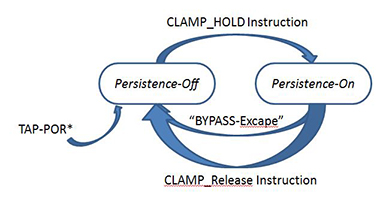
Figure 1. Persistence controller state diagram.
There are three new instructions introduced with these test modes: “CLAMP_HOLD”, “CLAMP_RELEASE”, and “TMP_STATUS”. The “CLAMP_HOLD” instructions set the TMP State to “Persistence-On”, while the “CLAMP_RELEASE” instructions will set the TMP state to “Persistence-Off”. The “TMP_STATUS” will read the status of the TMP controller.
ECIDCODE instructions. These instructions identify each individual compliant device by reading the ECIDCODE (electronic chip identification) unique for each die, which is like the serial number of each device. This will help the manufacturer identify counterfeit devices or identify a batch that has low yield during board testing, or even batch problems due to high field return.
Initialization instructions (INIT_SETUP, INIT_SETUP_CLAMP and INIT_RUN). This instruction initializes a compliant device into allowing programmable input/output (I/O) to be set up before a test is executed. This will help the manufacturing process by enabling a more robust test and prevent boards from internal damage that may occur when the devices under test (DUT) are not entered into a safe state.
IC_RESET instructions. This instruction provides reset functions in a compliant device through the test access port (TAP). The IC_RESET instruction permits control of the device system reset function during boundary scan testing.
Procedural Description Language (PDL). This is a new language for documenting the procedure of the new instructions introduced in this IEEE 1149.1 release. The PDL permits documentation of internal functions of the device, such as memory BIST (built-in self test) and permits it to be executed by the tool that supports the standard. Procedures and PDL samples are detailed in the IEEE Std 1149.1-2013, which can be downloaded from ieee.org.
The IEEE Std 1149.1-2013 is a big leap from the IEEE Std 1149.1-2001. The boundary scan testing of printed circuit board assembly (PCBA) and system testing will now be able to extend test coverage into BIST and other tests that were not possible with the previous revision.
IEEE 1149.6 (revision of IEEE Std 1149.6-2003). With the release of the IEEE Std 1149.1-2013 in 2013, it became necessary to update the IEEE Std 1149.6-2003 standard for boundary-scan testing of advanced digital networks to be able to adapt to the changes made in 1149.1. As of this writing, the 1149.6 working group is getting ready for balloting, and the latest changes are targeted to be released this year.
IEEE Std 1149.6-2003 mainly caters to testing high-speed differential signals which are normally AC-coupled. This type of signal is typically denoted by a coupling capacitor between driver and receiver (FIGURE 2). Prior to the formation of IEEE 1149.6 in the early 2000s, the netcom industries witnessed increasing demand for speed, which paved the way for increased use of high-speed differential signals on components, which in turn affected the testing of 1149.1 boundary scan, as this standard mainly catered to single-ended DC signal interconnection.
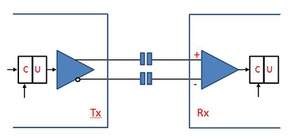
Figure 2. Differential signals with AC-coupling supported by IEEE Std 1149.6-2003.
Upon its release, 1149.6 was quickly adopted by netcom companies, component manufacturers and ATE (automatic test equipment) vendors.
The main focus for the 1149.6 working group is to include support of the IEEE Std 1149.1-2013 for the initialization process during testing and configuration of high-speed differential signals or AIO (advance input/output) test receivers and drivers using the PDL.
If history were to guide us, we can see that the adoption of the 1149.1 and 1149.6 standards were magnified when the netcom industry demanded new standards match their needs. This time, not only the netcom industry, but other industry segments, such as computing, infotainment and mobile computing, are demanding increased coverage of boundary scan to include access into the internal embedded instruments, as well as BIST during board or system testing, as they recover test coverage lost with the decreasing test access on printed circuit board assemblies.
IEEE Std 1687-2014. IEEE Std 1687-2014 is also known as Instrument JTAG ( iJTAG). The objective here was to develop a method and rules to access the instrumentation embedded into a semiconductor device without the need to define the instruments or their features using IEEE Standard 1149.1. The proposed standard would include a description language that specifies an interface to help communicate with the internal embedded instrumentation and features within the semiconductor device, such as built-in self test (BIST), embedded instruments that are normally accessible only to chip designers, as well as other internal functions of the device (FIGURE 3).
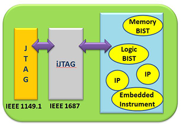
Figure 3. IEEE Std 1687-2014 connection to IPs and accessible through IEEE 1149.1 test access port (TAP).
IEEE Std 1687-2014 or iJTAG permits use of IEEE 1149.1 test access port (TAP) interface, which is prevalent on a majority of devices to manage the configuration, operation and collection of data from the embedded instrumentation circuitry inside the target device. The automatic test equipment (ATE) providers will be able to access the embedded instruments, logic BIST and IPs inside the device for chip, board or system testing purposes. The electronics manufacturers will be able to regain test coverage with minimal cost impact by integrating this solution into their current testing processes.
Adoption of IEEE Std 1687-2014 into mainstream testing will depend on how the industry responds. Each business segment is now waiting for a compliant device that will support the standards, and adoption will be based on their specific needs.
IEEE P1838. The IEEE P1838 proposal looks into the test access architecture for 3D packages that contain multiple die stacked vertically with through-silicon vias (TSV). The TSV technology enables stacking of silicon wafers or dies with vertical interconnections of each layer of wafer or die (FIGURE 4).
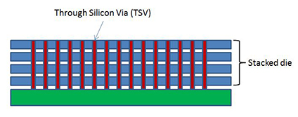
Figure 4. 3D package with stacked die using TSV.
Currently, IEEE 1149.1 and 1149.6 are the two most widely adopted standards in the manufacturing sector, and they support testing of interconnection of compliant device pins to other device pins. Multi-core or multichip packages are also supported, provided each die has the corresponding BSDL (boundary scan description language) that will permit the ATE software to determine the connection between devices. However, the internal connections inside the package are not part of the PCB netlist and will not be tested. The other challenge is that each die might be from a different vendor, and while each is tested separately as a single die as they are assembled as a single package, the interconnections between die are not covered by the existing standard test coverage (FIGURE 5).
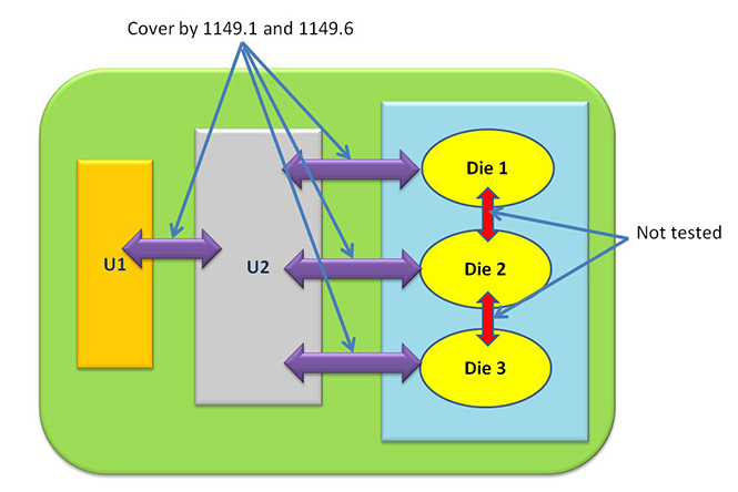
Figure 5. PCB with multi-core/multi-die package.
This gap in the coverage introduced by the current multi-core or multi-die package will further widen once 3D packaging gains wider adoption. The proposed IEEE P1838 will provide the standard for each die vendor to be compliant with the common standard, thus making way for both board and system tests to regain the coverage within the 3D package itself.
is a technical marketing engineer at Keysight Technologies (keysight.com); jun_balangue@keysight.com. The former Agilent Technologies Electronic Measurement Group is now Keysight.


