Clarifying Through-Hole Fill Levels

IPC-STD-001 is revising criteria for voiding and fill percentage.
In my September column, I spoke with Dave Hillman about IPC committee work on voiding guidelines for QFN central pad terminations. But he also told me the J-STD-001 task group increasingly receives requests from users for additional information and clarification of x-ray usage in other areas. This is because use of x-ray technology for analyzing solder joints has resulted in significant soldering process improvements. As with all technology introductions, however, the benefits and questions that result from the new information provided must be characterized, assessed and disseminated into practical form. One such area where x-ray technology has provided a tremendous amount of new information is plated through-hole (PTH) solder joints. The “insides” of these joints were previously “hidden” from scrutiny, unless subject to destructive methods, and the standards writers will need time to carefully revise old criteria to accommodate this new information. With this in mind, IPC formed a task group (called Team Skeleton) to discuss this and other matters, with the goal to develop additional x-ray-related guidelines and requirements for inclusion in future IPC documentation. As usual, Dave says, “All are welcome to participate and provide their comments and suggestions.”
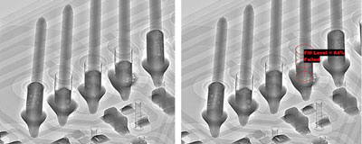
At present, through-hole joint fill requirements and inspection criteria are commonly identified and understood within the J-STD-001/IPC-A-610 specifications. Those indicate Class II/III assemblies should have at least 75% fill, based on the through-hole depth. An oblique angle view x-ray clearly shows the nature and depth of the fill nondestructively (FIGURE 1). Additionally, many x-ray systems offer software that indicates the fill level percentage (Figure 1, right). However, as I have said before, these measurements have a degree of error. As an alternative, simple operator examination can quickly determine what is obviously acceptable and unacceptable, with any subsequent measurement used for clarification in the subset of “not sure” joints. If you are “not sure,” and the fill is around the 60 to 80% level, is it not worth flagging a process issue indicator, even if the actual value is within specification requirements?

Figure 1. Plated through-hole joints (PTH) with varying levels of fill percentage. All joints show the presence of some voiding. The right image shows the fill calculation possible on some x-ray inspection systems.
While that situation probably covers the most likely issue to befall through-hole joints, the task group suggests further clarification be added to cover more eventualities and better define what is and is not acceptable. In particular, it should clarify the implications if and where voiding occurs within the solder-filled portion of the joint, even if it is not 100%-filled. Further, the location of the absent fill material within the joint should be discussed, if it was not present at one end.
On the presence of voiding within the filled section of the joint (Figure 1), the task group suggests voiding inside these solder fillets is not unusual, and therefore any calculation of the level of voiding should not be subtracted from the fill percentage value.
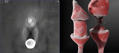
On the location of the “missing” fill material, the task group suggests, when assessing solder fill in PTH joints (per J-STD-001, section 6.2 and Table 6-6), to define a “circumferential solder separation” to explain the missing fill (void) area and its location within the joint. This definition would be classified as an internal void in the solder fillet extending around the entire circumference of a plated through-hole and lead/wire. In other words, there is no continuous flow of solder between the solder-source side fillet and the solder-destination side fillet. Therefore, when using x-ray evaluation to assess solder fill percentage in plated through-holes, a continuous solder fill should be evident from the solder-source side toward the solder-destination side, even if it is not 100%. The proposed J-STD-001 requirements would not permit any continuous circumferential solder separation between a solder-source side fillet and a solder-destination side fillet (FIGURES 2 and 3).

Figure 2. X-ray image of two PTH joints. One joint has 100% fill but also includes a void. The other includes a circumferential solder separation and would therefore fail the proposed criteria.

Figure 3. PCT reconstruction of the joints shown in Figure 2. A reconstructed 2-D x-ray slice through approximately the middle of the joint depth is shown on the left, and a 3-D representation of both joints is shown on the right.
Figure 2 shows one PTH (left) with 100% fill but also containing a void. This would still be considered 100% fill, and the voiding level would not be subtracted. The other PTH (right), however, has solder at the top and bottom but none in the center, thereby failing the proposed criteria, and is markedly different in shape from the joints shown in Figure 1, where the fill extends from one side but does not reach all the way to the other. Figure 3 shows the same joints as in Figure 2 but through a nondestructive PCT examination. A reconstructed 2-D x-ray slice shows the presence and absence of solder around the respective leads at around the middle of the joint depth. A 3-D representation of the joints is also shown.
This is the current proposal. It helps define acceptable and unacceptable PTH joints and considers whether missing fill material lies between board and device, rather than just from one end, and explicitly indicates any voiding within the filled portion should not be included in any fill percentage calculation. If adopted, these clarifications will be included in future IPC document revisions. Contact the J-STD-001 Team Skeleton Task Group if you prefer otherwise.
Au.: Images courtesy Peter Koch, Yxlon International.
, is an expert in use and analysis of 2-D and 3-D (CT) x-ray inspection techniques for electronics; dbc@bernard.abel.co.uk.
Press Releases
- Altus Partners with Sellectronics to Enhance Manufacturing Capabilities with PVA Delta 8 System
- ITW EAE Celebrates Major Milestone in Domestic Manufacturing Expansion
- Micro Technology Services Selects PBT Works CompaCLEAN III for Advanced PCB Cleaning Performance
- Indium Corp. is Electrifying the Future with Advanced Materials Solutions at Productronica


