

2013 Articles
A review of four case studies of product conversions.
With the next RoHS compliance deadline approaching in July 2014, many electronics manufacturers that were exempted from the 2006 mandate will soon be forced to comply.
The initial conversion of consumer and other electronics was painful and costly at all levels of the supply chain. But over the past six years, many valuable lessons have been learned that can ease the transition for the next wave of products pursuing compliance. Furthermore, the higher reliability products with longer lifecycles typically use older packaging and PCB technology, and therefore are excellent candidates for cost reductions as their designs are updated.
Keys to a successful, economically advantageous conversion include thoroughly reviewing the product’s design, identification of cost-reduction opportunities and allotting adequate time for testing and qualification.
The first step in any RoHS conversion activity is a thorough analysis of the product’s bill of materials (BoM). The BoM should be reviewed, or “scrubbed,” for availability of RoHS-compliant components, for compliant components that are or will soon become obsolete, and for opportunities to transition through-hole (PTH) component to surface mount (SMT).
The BoM scrub will indicate one of three situations:
1. Complete set of RoHS-compliant parts are available.
2. Some parts are not available as RoHS compliant.
3. Some parts are not available as RoHS compliant, and others face obsolescence issues.
Each scenario requires different actions to complete the product conversion.
If a complete set of RoHS-compliant components is available, the conversion is very straightforward and relatively easy. The BoM is updated, and a design for manufacture (DfM) review is conducted. The primary purpose of the DfM review in this situation is to update the land patterns for Pb-free processing using the original PCB layout. The layout is updated to reflect the new footprints and, whenever possible, incorporate other DfM opportunities identified in the review. After the layout is updated, the fab drawing is then updated to indicate the new RoHS-compliant material and process requirements.
The product with the updated BoM, layout and fabrication drawing gets prototyped, tested and validated using standard manufacturing processes and practices. Following validation of the compliant product, final documentation is prepared and production is started. With the fully RoHS-compliant assembly now in production, the conversion process is considered complete.
If a complete set of RoHS-compliant parts is not available, the process requires several extra steps that take a little more time and cost a little more money. Alternate components must be researched, selected and approved. In some cases multiple parts may be required to satisfy the functional requirements of the unavailable components. A new BoM must be generated, and when complete, a DfM review is conducted. Because the new BoM will likely require a new PCB layout, more DfM opportunities may be incorporated during the re-layout phase. The new PCB design will dictate a new fabrication documentation package.
With the added steps of identifying new components and the new PCB layout complete, the conversion process now follows the same path as the product with simpler updates. It is prototyped, tested and validated. Then the final documentation is prepared, production is launched, and the conversion is finalized.
If a complete set of RoHS-compliant parts is not available and component maturity or obsolescence issues signal the need for redesign, the conversion process again requires more added steps, time and cost. Alternate components are identified, a new BoM is generated, and a DfM review is conducted. However, eliminating the antiquated or obsolete components may require major mechanical, electrical or electronic redesign. The new design will also need a complete new set of documentation.
As with the other two conversion situations, the design now progresses through the same prototype, test and validation phases; the final documentation is prepared; production is begun, and the process is completed.
Figure 1 depicts the RoHS conversion process and outlines the key engineering activity in the green boxes. Every conversion starts with a thorough BoM scrub. This is arguably the most important part of the conversion process, as its results determine the conversion path. Failure to identify exact drop-in replacements or impending obsolescence issues at the earliest stage can result in expensive setbacks and course corrections at later stages of the project.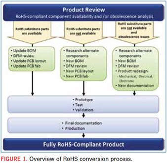
Every conversion concludes with the same activities: prototyping, testing, validating, documenting and producing. Depending on the end-use of the product, testing and validating times can vary dramatically. When planning to meet conversion deadlines, validation requirements should be carefully considered.
In between the BoM scrub and the prototype build, a lot of engineering takes place. The following four case studies describe the key engineering activity in each conversion process.
Case 1: Remote display keypad for medical device. Figure 2 shows before and after images of a medical manufacturer’s device user interface module. This is an example of an extremely simple RoHS conversion. The BoM scrub indicated that all but one part was available in Pb-free surface finish, and the one missing component was easy to replace. The scrub also identified a major cost reduction opportunity: updating the PTH transistors to SMT packages. The SMT components are less expensive than the PTH ones, and the SMT assembly process is far more cost-efficient than PTH assembly. The new components fit within the footprints of the previous components, so updating the layout was fast and easy.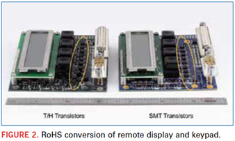
The savings achieved by the SMT migration completely offset the higher costs of Pb-free PCBs, components, and assembly. The net savings on the RoHS-compliant product was 2% per assembly. While this is not considered a substantial cost reduction, it is still far preferable to the anticipated cost increase.
Case 2: Analytical equipment controller boards. Before and after images of an industrial controller assembly are shown in Figure 3. This conversion required a replacement module with the exact same interface and functionality as the original to guarantee seamless integration into the final product. The BoM review indicated that the age of this product and its extensive use of PTH components offered multiple opportunities for cost reduction through redesign:
- Conversion of PTH to SMT components reduced main board area by 40%.
- Relocating opto-isolator to main PCB eliminated daughter card assembly.
- Reducing the component count and cost reduced the total BoM cost.
- PTH to SMT conversion reduced labor cost.
- Electrical redesign reduced cost of major components by using new, higher-capability processor chips. Logic and motor controls were consolidated into one processor, which also performed hardware control functions that were previously executed externally.

The reduction in PCB and manufacturing costs, and the benefits of component consolidation resulted in an overall savings of 31% per assembly.
Case 3: Real-time clock. The RoHS conversion of the real time clock and RAM backup module shown in Figure 4 was driven primarily by obsolescence. When faced with component obsolescence, the easiest option is often to purchase enough components to supply the product through the end of its lifecycle. In this case, however, the lifetime buy was not a viable option because the product had 10 years left in its lifecycle and required a five-year shelf life. The old modules were manufactured with internal batteries that would last at least five years but nowhere near 15 years.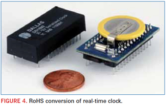
The new design had to address battery life issues and meet FDA requirements. Because the only alternative was complete redesign, RoHS compliance was added to its list of specifications. The redesign incorporated the following features:
- RoHS compliance.
- Battery installed at time of shipping final product, maximizing its shelf life and enabling easy replacement in the field.
- The exact form, fit and function of the new component exempted it from FDA recertification, saving the medical device manufacturer additional resources, time and money.
In addition to this redesign achieving RoHS compliance, extending the shelf life of the product and minimizing regulatory expenses, this conversion reduced the cost by a staggering 52% per assembly.
Case 4: Embedded process control board. Like Case 3, the conversion of the controller boards shown in Figure 5 was also driven by component obsolescence. These assemblies had two obsolete components, and more pending. One of the components was sourced through brokerage at 8X its original price! And like Case 2, extensive use of PTH technology made this a perfect candidate for redesign, even if the obsolescence issues were not considered.
Cost-reduction activities on this product included:
- Elimination of expensive, obsolete components.
- Consolidation of two PCBs into one using modern devices and fewer discrete parts.
- Addition of self-diagnostics to reduce test time by 66%.
- Fewer PTH components and more SMT components to improve manufacturing efficiency and reduce labor costs.
In addition to reducing cost, the redesign added functionality. It afforded the opportunity to incorporate new features requested by the customers, which included:
- Adding a USB port.
- Providing a more sophisticated communications protocol.
This conversion combined two PCBs into one, lowered the parts count, reduced test time and added functionality, while reducing product cost by 36% per assembly.
Strategies for Cost Reduction
Many factors influence the total cost of an electronic or electromechanical assembly, and most of them are interrelated. During the BoM scrub, the engineering team should look for opportunities to:
Reduce PCB size or count. PCB area and layer count are the biggest factors in PCB cost. Reducing area, which may be achieved by component count reduction or replacement of PTH with SMT components will reduce the PCB cost. Reducing layer count by using finer line spacing can also reduce PCB cost. And eliminating a PCB eliminates its cost completely.
Reduce parts count. Lowering the parts count usually lowers the total BoM cost. It can also shrink the PCB area requirement, improve manufacturing efficiency, and reduce labor/overhead/handling costs.
Reduce parts cost. Obsolete components are always more expensive than current ones, and mature, PTH components are almost always more expensive than modern SMT ones. Updating package types can save money; even older SMT packages often cost more than newer ones. Using up-to-date components that can combine multiple functions reduces parts cost, parts count, and PCB area requirements.
Convert PTH to SMT. As previously discussed, SMT parts are almost always less expensive than PTH parts; they require less PCB area, offer significantly better manufacturing efficiency, and reduce labor requirements.
Because the cost-drivers are so deeply interrelated, incremental design changes can generate substantial savings.
Discussion and Conclusion
While RoHS-compliant electronics products require more expensive PCBs, components and manufacturing processes, updating noncompliant products can actually save money. Electronics packaging and manufacturing technology progresses at such a rapid pace that updating the design of a legacy product using modern technology may reduce its cost, despite the typical price premiums associated with Pb-free soldering and other RoHS requirements. Many of the electronic assemblies facing the 2014 compliance deadline are excellent candidates for cost reduction due to their age and technology levels.
Four cases of RoHS conversion were presented, ranging from the simple BoM and footprint updates to complete redesign. Each project followed different conversion paths and employed different combinations of cost-reduction strategies, and all of them were more cost-efficient than their pre-RoHS ancestors.
The answer to the title question is yes, it is possible to reduce cost when converting electronic products to RoHS compliance. Overall cost-reduction depends on the age and technology level of the product. Keys to successful cost-reduction efforts include a thorough BoM scrub to help define the conversion path, a component consolidation strategy, incorporation of DfM recommendations, and consideration of testing requirements for validation and qualification.
Ed.: This article was originally presented at SMTA International in October 2012 and is published here with the permission of the authors.
Philip DiVita, David Steele and John Kanavel are with Da-Tech Corp. (da-tech.com); pdivita@da-tech.com. Chrys Shea is founder of Shea Engineering Services (sheaengineering.com); chrys@sheaengineering.com.
As manufacturers take care to wash traces of so-called Conflict Minerals out of their supply chains, many citizens of the Democratic Republic of Congo have been deprived the opportunity to live a better life by mining the precious ores beneath their feet. A small but growing group of major electronics OEMs and suppliers, together with the Dutch government, are working on a plan to ensure certain mines under the protection of the national army are certifiably “conflict-free.” One of those suppliers is Alpha. CIRCUITS ASSEMBLY editor in chief Mike Buetow spoke by phone with Alpha vice president of global marketing & corporate development Bruce Moloznik about the new initiative.
CA: What can you tell me about the Conflict-Free Tin Initiative?
BM: We are in fact part of that. We have been talking to people about the issue and going forward with what is hopefully a unified approach. In fact, we are involved in a lot of groups on the conflict minerals issue: the GeSI-EICC (auditor certification scheme), the CFS (The Conflict-Free Smelter Program), and the reporting template, where suppliers can identify where they get their tin. Let me clarify a few things about this, by the way. Conflict minerals are the minerals that tin, tantalum, tungsten and gold as a category are derived from. Conflict tin refers explicitly to tin from an illegal mine. The SEC rules cover any public company that uses tantalum, tin, tungsten or gold. The concern, and the reason this pilot is being put in place, is one thing: Will this work?
CA: How did Alpha get involved in the CFTI?
BM: We’ve been involved from early on in the pilot program, which was over a year ago. We drafted our policy and implemented it at the beginning of 2012. We strongly believe we have been offering conflict-free minerals since we became aware of the issue, but we ask all our suppliers to warrant they are not trading in conflict tin.
A lot of companies, in doing their audits, are looking at what their suppliers have done. The actual SEC SD (Supplier Declaration) is one page. If you find out your tin comes from the Congo, there’s a whole additional level of due diligence. The easiest thing for suppliers to do is to avoid it. But these minerals are the only assets the Congo has. The worst thing is the unintended consequence of a soft boycott on tin.
CA: When will the program begin?
BM: Our focus now is to get the first proof of concept through. There are many potential areas of cost increase involved throughout the supply chain. If all of the tin we needed to buy could be purchased conflict-free starting Jan. 1, this could be a smooth transition. But, I think this is going to be like lead-free, where companies will slowly transition and only then when forced to from the top of the supply chain. The addition, recycled material being allowed without the requirement of the original country mine of origin, was critical for the law to be implemented. This was based on the pervasive use of recycled material in our industry. The reporting period begins Jan. 1, 2013, and the only businesses that have to do this are US public companies, but, for example, for Asian companies that sell to public companies, the US company’s due diligence will rely on their supplier’s due diligence, who actually purchases the tin-containing material.
If yours is a smaller US company, and none of your goods are sold into public companies, you won’t be affected. There are certain European companies that will piggyback on this law. Europe won’t be insulated, but it will be voluntary. By the end of 2013, these companies will have to put together all this due diligence to prove what they did to keep conflict tin from their supply chain. Not all smelters will be certified as of Jan. 1, and some may never get certified.
CA: How is mine security handled for the pilot?
BM: The smelter is the supplier that buys directly from the mines and is transparent about having bought from the DRC. This partner smelter is in the process of getting their Conflict Free Smelter certification. ITRI is a key player in putting this pilot together on the ground. They are involved with others in the “bagging and tagging” cassiterite with a seal that indicates the Source Mine of the material is a conflict-free mine. That bag’s contents will be transferred to a consolidator and sold to the smelter and smelted with other conflict-free tin. Alpha will buy this certified conflict-free tin, and we will not cross-contaminate it with other mainstream sources – to make conflict-free finished goods.
CA: Does it make economic sense today to buy conflict minerals?
BM: It is unclear what will happen to price. When you buy metals, you buy at the LME (price), plus traders’ fees, shipping and freight. We’re going to have to demonstrate the value customers are getting. Even if every smelter in the world could suddenly on Jan. 1 provide conflict-free tin, Alpha will still need new labels, new traceability IT systems, and have other costs that will increase our cost base in an already extremely price competitive environment.

Custom nozzles can reduce processing time and improve selective soldering machine flexibility.
Somewhere between the polar opposites of point-to-point selective soldering and mass solder dipping lies a unique happy medium known as stamp soldering. Stamp soldering in fact is a rather broad term, but what I’m talking about here is something of a middle ground between the two: an offbeat type of stamp soldering that can be achieved with a conventional selective soldering machine and that saves a tremendous amount of processing time while actually extending or expanding the flexibility of the conventional selective soldering machine.
The basics of conventional selective soldering are known to most. A single nozzle mounted on a solder pot and fountain travels around the underside of a PCB, soldering specific sites according to an individual sequential program created for that board. This method is very flexible and permits rapid changeover between products. However, the time it takes (TAKT) to process that board in its entirety, and each successive one, is a direct function of the number of solder sites on that board and the dimensions of the board itself. For example, a single board, as large as 18" square with 500 solder points might take as long as 5 to 7 min. to process, since each point must be soldered individually.
At the opposite end of the spectrum is the mass solder-dipping technology (conventional wave), which isn’t actually dipping at all but involves the use of custom fixtures and various forms of masking over a solder fountain source; the fixture has apertures to match the solder points on the PCB, which again could be as large as 18" square. All the solder sites on that board are replicated in a large solder wave. Expensive robotics position the board and fixture over the fountain/wave for a preset dwell time, after fluxing and preheating, and the PCB is soldered all at once. This latter method is suitable for very high-volume soldering and speed, for a fast TAKT time; that 18" square PCB might take only 10 sec. to process versus 5 to 7 min. the conventional way. However, the setup is dedicated to just one product and is quite difficult to change to a different product. The equipment is costly, as are the individual custom soldering fixtures. This method is also known as stamp soldering, but it is different from the “middle ground” that we discuss here.
Our middle ground stamp soldering can be accomplished using a conventional selective soldering machine fitted with a special stamp soldering nozzle. Granted, it’s a much smaller fixture than the one needed to mass solder a large board; in fact, the one shown in Figure 1 has only four apertures or nozzles mounted on it. It is a custom fixture designed for a specific board. The rectangular or longitudinal aperture is for a connector; the larger round aperture is for a round cluster of pins, and the two miniature twin nozzles are for soldering adjacent LED components. In a panelized PCB scenario, the custom nozzle indexes around from board to board and stamp solders that small pattern on each PCB. The nozzle can also be removed and exchanged simply with a standard nozzle for ordinary selective soldering routines.
The advantage of this nozzle is that it processes every board in the panel in exactly the same fashion vs. the mass technique that strikes all solder joints at once. So, the “selective stamp nozzle” is somewhere between the mass solder dip machine, which is very expensive and highly dedicated, and a conventional selective soldering machine, which is flexible and non-dedicated. This is actually a hybrid, with the only dedicated part being a small custom multi-port nozzle. When aperture sizes vary, to maintain uniformity of pressure and flow in all the apertures, threaded set screws are installed for each aperture so that the flow can be restricted or constricted in order to achieve balance.
In process, a dropjet fluxer applies flux only where it is needed, and if necessary, the board is preheated. The board is positioned, checked with fiducials to make sure it’s in place, and then the solder pot, with its pumped aperture, comes up and contacts all the solder sites at once, effectively making the solder joints, and then drops out of the way under programmed control.
This pattern could, of course, be sequentially soldered using a single nozzle, with the time needed to solder the entire pattern estimated at about 40 sec. Using the custom stamping fixture in a step and repeat sequence, all points might be soldered in 6 to 7 sec. If several hundred identical boards are to be soldered, the cumulative time savings become readily apparent. Perhaps the most significant aspect of this higher throughput rate is that it can be achieved using a run-of-the-mill, affordable selective soldering machine without any costly adaptation.
Alan Cable is president of A.C.E. Production Technologies (ace-protech.com); acable@ace-protech.com.

Press Releases
- Orbit Technologies accelerates growth and doubles production capacity with Europlacer iineo placement machine
- CE3S Brings Back Free ANSI/ESD S20.20 Training Series This August with Desco Industries
- Green Circuits Names Adam Szychowski Chief Revenue Officer
- MicroCare Appoints Doug Kay as Director of Market and New Business Development