

Hidden Trouble in a BGA Package
Does a small node suggest anomalies – and potential failure?
A small raised area was initially noted on the top surface of the plastic ball grid array (BGA) package discussed here. To learn whether there were other structural anomalies deeper within the package, it was imaged by both x-ray and ultrasound. The x-ray imaging was performed first, using a Nordson-Dage Quadra 7. When traveling through a sample, the x-ray beam is locally attenuated by the density and thickness of the material through which it passes. Very dense materials such as metals may limit the thickness of the sample that can be imaged, while materials such as plastic are far less attenuating. The completed x-ray image reveals in very high-resolution local changes of attenuation over the area being imaged.
FIGURE 1 shows one corner of the BGA’s die and the attached wires. All the wires are intact here and on the rest of the BGA. All features are encased in the nearly transparent (to x-ray) mold compound. The black circular features are the solder balls under the BGA. The indistinct gray fea-ture just above the edge of the die is caused by the variable thickness of underfill material extruded from beneath the die. Within the area of this image there could be delaminations or voids – i.e., air-filled gaps – on top of the die or in the die attach material below the die, but air attenuates an x-ray beam so slightly, and the gaps are typically so thin, that these gaps would not be imaged.
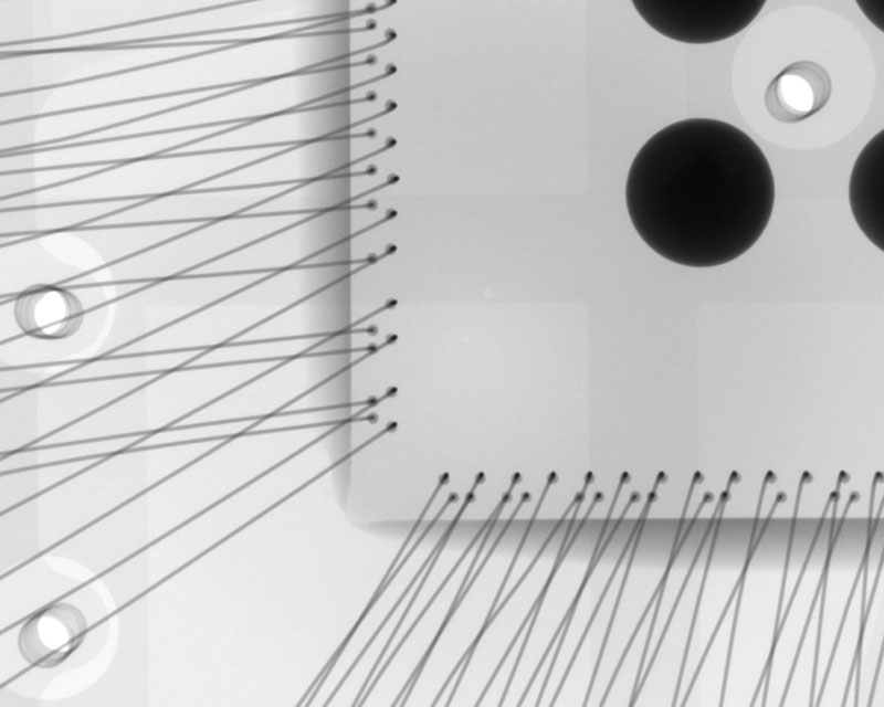
Figure 1. X-ray image of one corner of the BGA package reveals no broken wires.
The acoustic micro imaging tool, a Nordson-Sonoscan C-SAM, was then used to image the BGA. FIGURE 2 shows the topography of the BGA package but no internal features. In this viewing mode, the transducer emits a pulse of ultrasound and accepts for imaging only the first echo from each of the thousands of x-y locations. This mode is frequently used on components such as BGAs where surface irregularities can indicate internal structural irregularities that may cause elec-trical failures. Ultrasound was pulsed at the surface of the BGA package in single tiny pulses, emitted by the moving transducer that is coupled to the surface of the package by an accompanying water column. The speed is high: The moving transducer can launch and receive echoes from tens of thousands of launched pulses per second. At each x-y location, the pulse is launched and its echo received before the transducer images the next location. A completed acoustic image may contain thousands or even millions of pixels, each the product of an echo from one pulse.
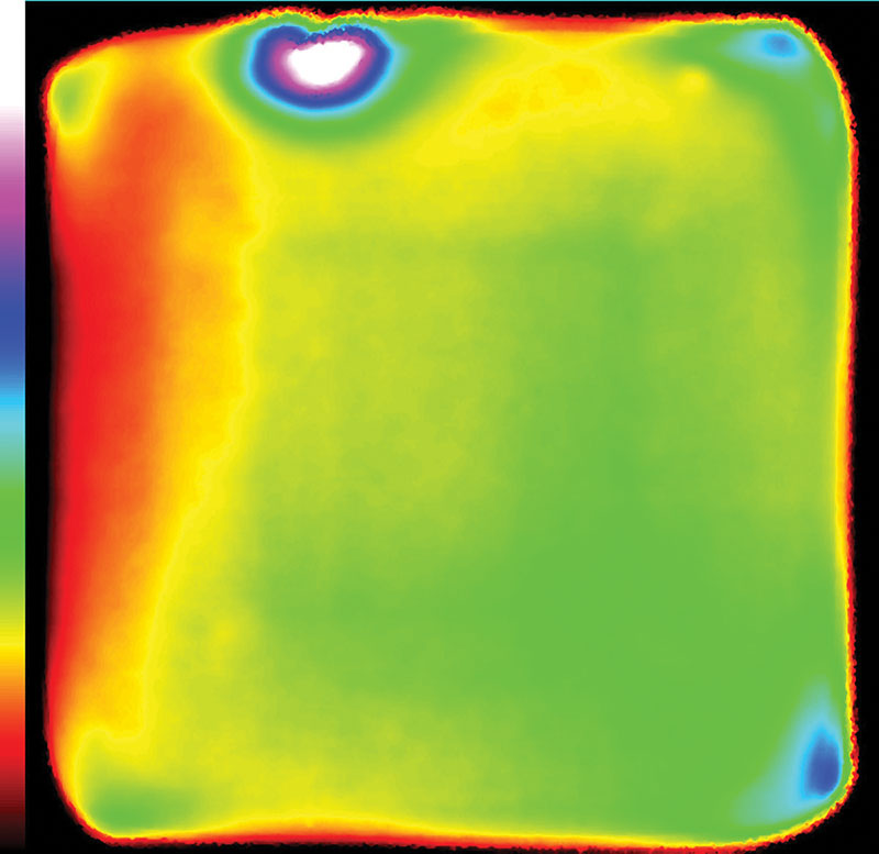
Figure 2. Acoustic topographic map of the BGA package surface. White points are highest; red-black points are lowest.
To make a topographic map of the surface of the BGA package, the acoustic micro imager software first recorded the arrival time for the first echo to arrive at the transducer from each x-y location. The surface of the BGA package is not flat. The earliest arriving echoes were imaged with white pixels. In Figure 2, such echoes are found only at the highest portion of the surface bump near the top left of the image. Echoes arriving next were colored magenta and surround the white area. The next arrivals were made dark blue, and so on.
The color map used to make this image is at left. White – the color of the first arrivals – is at the top of the color map. Next is magenta, then dark blue, then green, and so forth. The lowest portions of the package’s surface are red-to-black pixels at the edges. The difference in altitude between the highest and lowest points on the surface is approximately 0.25mm.
FIGURE 3 used an interior imaging technique that is probably the most commonly used acoustic mode. A gate is first decided on, a defined vertical depth within the part. Only echoes reflected by material interfaces within this gate are accepted for imaging. Echoes are ignored if they were re-flected by material interfaces above or below the gate. Vertically, the gate can be as wide (vertically) or narrow as desired, even down a tiny fraction of a micron. Here, the gate’s width is approximately 0.732mm, extending from near the surface to the tops of the wires.
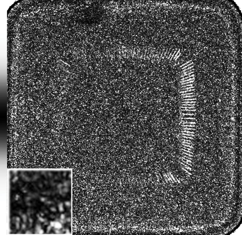
Figure 3. Gating echoes on a thin slice just above the die shows the die is tilted.
Two items are of interest. The first is a darker spot near the top edge of the image, just left of center. At first glance it might appear the mold compound is much denser here, but that is very unlikely. But the dark spot is also positioned directly below the excess mold compound on the surface.
What is happening is this: Ultrasound is pulsed into the BGA and reflected by material interfaces, including interfaces between the filler particles and the mold compound. The ultrasound is also somewhat attenuated simply by traveling through the mold compound. Ultrasound striking this dark area had to travel through the bump on the surface of the package twice, going to the gate and returning as an echo to the transducer. Because it traveled through more mold compound than in surrounding areas, it is more attenuated than surrounding areas, and the area of the bump appears darker than the areas around it.
The dark area closely resembles the shadow that would be cast by an air-filled void of this size higher in the package. Even if an air gap is extremely thin, the air-to-solid interface at its top reflects virtually all an arriving pulse back to the transducer. None of the ultrasound crosses the interface, so an image of a lower interface will show the dense black sharply outlined shape of the gap.
The inset at lower left shows the southeast portion of the dark area magnified. Two details prove it is not the shadow of a void: First, it contains white reflections from filler particles within this gate; second, the border of the dark region is not sharp.
The second item – the fine white lines in the image – could be more serious. The lines are the loops of wires running from the die to nearby lead fingers. The interface between the mold compound and the metal creates a high amplitude echo imaged in white. White is at the bottom of the color bar at left.
The tops of the wire loops appear along the right side of the die and along the righthand portions of the top and bottom. To the left of these areas, they are missing because the tops of the loops are below the bottom of this gate. The defect is not with the wires but with the die they are attached to, which is tilted downward to the left. Such tilting puts mechanical stress on many of the wires and makes eventual wire breakage and field failure more likely.
The die face itself is shown in FIGURE 4. The die is tilted, but the gate used here was wide enough vertically to accommodate the entire depth range used by the surface of the die. Some of the wires are faintly visible around the edges of the die.
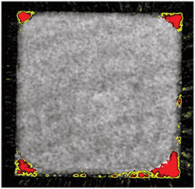
Figure 4. Red mark delaminations of the mold compound from the die at all four corners.
The problems here are obvious: the red areas at each of the corners. These are disbonds between the mold compound and the die, which reflect nearly 100% of the arriving ultrasound as a powerful echo. The two materials on either side of the gap have different coefficients of thermal expansion, with the result that the heating and cooling of normal operations will encourage the cracks to grow and break wire bonds. The x-ray image of one corner of the die in Figure 1 showed no broken wire bonds. Air gaps were present when the x-ray image in Figure 1 was made, but the attenuation of the x-ray beam by an air gap that may be only a few microns thick is negligible, and there was no trace of an air gap in Figure 1. Because no wires are broken, this BGA might pass an electrical test at this point.
The bottom portion of FIGURE 5 includes much of Figure 4, but with a white horizontal line near the bottom of the image. The line marks the path along which the transducer repeatedly scanned back and forth. On the first scan, it accepted echoes only from a very narrow gate at the base of the die. It moved very slightly upward to scan back, collecting any echoes from that narrow gate. When it reached the surface of the part, the scans were in effect stacked on top of each other to give a nondestructive cross-sectional view of the package along the white line. The blue arrow connects the two views. (The two red delaminations seen in Figure 4 at this location have been removed to show this sectioned view.)
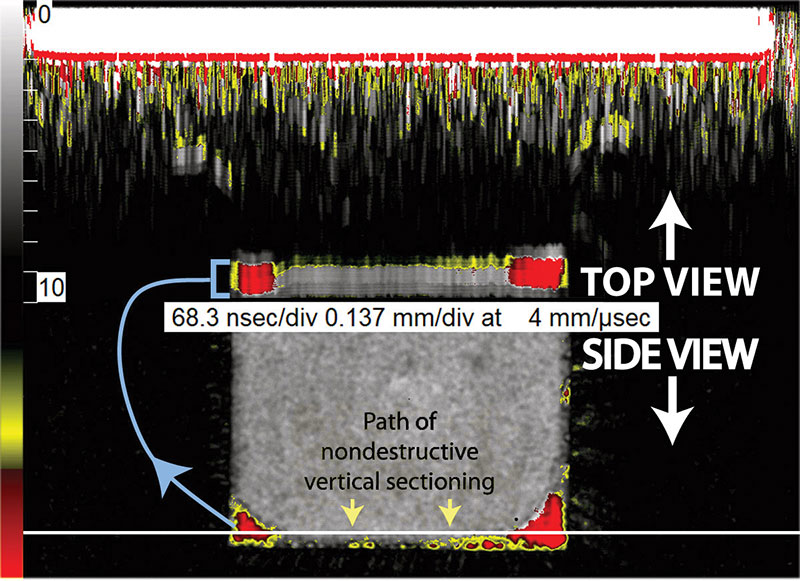
Figure 5. Bottom half: location of path for cross-sectional scanning. Top half: resulting cross-sectional view.
There are no surprises in the cross-sectional quantitative B-scan analysis mode (Q-BAM) view: The delaminations are present, and no anomalies are not seen in the planar view. The yellow flecks present higher up in the Q-BAM image are filler particles added to plastic to create the mold compound mixture.
To sum up: This BGA package has an uneven top surface, which might cause a handling problem during assembly. X-ray shows no broken wires, although the tilted die could cause wires to break in the future. Most seriously, at each of the four corners of the die are delaminations capable of ex-panding over time and shearing off wires.
is a consultant with Nordson Sonoscan (nordsonsonoscan.com); info@nordsonsonoscan.com.


Press Releases
- Javad EMS Upgrades Through-Hole Soldering Capacity with New SEHO PowerWave System
- Sharpen Your Selective Soldering Skills with Kurtz Ersa's July VERSAFLOW 4/55 Training
- Omron Advances Inspection Technology with NVIDIA Omniverse and Metropolis
- Seika Machinery’s SMI 2026 Webinar Series Continues with Focus on PCB Cleaning Before Solder Paste Printing