

News
News
Using a Printer in Chip Attachment and Encapsulation
Part two of a look at how traditional SMT processes address semiconductor packaging.
In our November column, we began this two-part discussion on the use of SMT processes to address semiconductor packaging. In this conclusion, we cover chip attachment and encapsulation.
Attaching the chip. Bumping at chip level enables the die to be attached to the substrate either by direct chip attach/flip-chip on board or, as in this case, flip-chip in package. These processes all require the chip to be mechanically and electrically bonded to the substrate.
The chip is interconnected by solder bumps on the die collapsing in a controlled manner to form a soldered joint between the solder pads on the chip and substrate. Before the placement of the chips, a very low activity flux is applied on the substrate to provide tackiness and prevent chip movement. This application of flux can be achieved by either flooding the entire area (Figure 1) or printing the individual pads (Figure 2). The choice is based on individual preference. The assembly is then reflowed until the solder bumps form an intermetallic joint between chip and substrate.
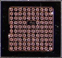 FIGURE 1: For direct chip attach applications, flux can be applied through flood printing ... |
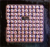 FIGURE 2: … or applied directly to the lands (site printing). |
The addition of an underfill material compensates for any coefficient of thermal expansion mismatch between silicon die and substrate, and can be applied afterward using a capillary formulation. An alternative method is to apply a no-flow material at the wafer level.
Encapsulation. Once the chip has been placed within the package, the printer can be used to encapsulate the package. As a low-cost, high-volume alternative to injecting molding and dispensing processes, a stencil-applied overmold technique combines the application of unique liquid encapsulant compounds with printing technologies. When applied using enclosed print head technology, the single component, silica-filled liquid encapsulant provides a smooth surface and void-free molded package appearance.
In this process, encapsulant material is applied through either a 3-D stencil or metal mask, depending upon the specific application. This aids productivity and design flexibility, and reduces capital tooling and maintenance costs compared to injection molding.
The enclosed transfer head is fitted with an overmold-filled cassette, pressure is applied and the overmold is forced through the transfer head to fill the stencil apertures (Figure 3).
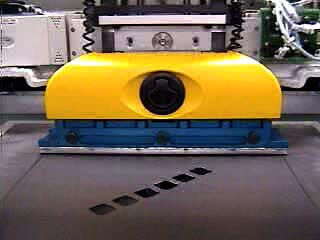 FIGURE 3: Enclosed print head applies encapsulant material to overmold the package. |
Coated blades create a tight gasket seal between stencil and substrate, ensuring repeatability and a good surface finish. The material is then cured and the encapsulation material is solidified (Figure 4).
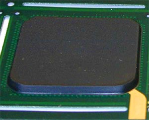 FIGURE 4: Encapsulation is complete. |
Finally, while cost and productivity now enable the daily use of screen printers in packaging applications, the equipment is expected to meet future demands brought on by higher I/O counts and finer interconnect pitches, plus the shift to Pb-free.
Clive Ashmore is global applied process engineering manager at DEK (dek.com). His column appears semimonthly.


Press Releases
- Altus Group Invests in Major Headquarters Expansion to Showcase Complete Turnkey Manufacturing Capability
- ViTrox Americas Welcomes Eric Cruz as Technical Support Engineer
- ECD Strengthens Engineering Team with New Software Development Hire
- ViTrox Americas Welcomes Doug Ennis as Senior Field Applications & Service Engineer