

2005 Articles
Beyond Assembly
Alternative applications for high accuracy screen printing.
In my first column I promised to address some of the ways that high-accuracy mass imaging is enabling processes beyond traditional assembly. We have only touched the tip of the iceberg and are discovering new applications for this technology everyday. This month I will discuss some of these processes.
Because high-accuracy mass imaging is not a serial process, it offers compelling economic advantages in a variety of medium- and high-volume assembly and packaging applications, especially ones that have traditionally used dispensing techniques.
First, let’s look at wafer bumping. In this process, mass imaging is used to apply solder deposits to the base of the silicon die, which are then reflowed to form balls of 100 to 300 µm pitch (Figure 1). The die can then be placed directly face down onto the substrate as a flip chip on board or direct chip attach or assembled as a flip chip in package such as a BGA or CSP. This technology enables the massive increases in microprocessing speeds due to shorter communication paths involved and improves throughput dramatically.
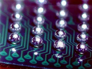 |
| FIGURE 1: Solder deposits applied to the base of the die, then reflowed to form balls. |
Wafer bumping is not the only semiconductor packaging process that this technology enhances. Mass imaging techniques have also been used successfully for fluxing, sphere placement, encapsulation and substrate bumping.
One well-known chip manufacturer needed to increase throughput and was hesitant to purchase additional dispensers to achieve the required production rate. The company had historically dispensed every material used in its process: flux, underfill, thermal interface, lid seal and even solder paste. Their reasons: the need for precise alignment of singulated substrates within a carrier, maintaining extreme cleanliness, and the challenge of depositing materials onto partially populated substrates.
To increase throughput, the company turned to mass imaging technology as an alternative to dispensing. The primary bottleneck – solder paste deposition for passive attach – was the first to be addressed. A new tooling solution was used that resolved the alignment accuracy issue and permitted precise, automated alignment of substrates within carriers (Figure 2). The tooling system is comprised of a precision pin design and a matched vacuum tower that centers each substrate with the JEDEC-compliant carrier and then lifts them to the printing position. This technique achieves the effect of a virtual panel consisting of up to 60 independently aligned substrates and it solved the company’s throughput and precision issues.
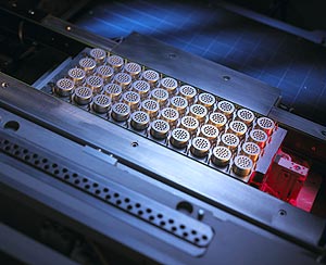 |
| FIGURE 2: A novel tooling method that auto-aligns substrates within carriers. |
Substrate bumping also benefits from mass imaging techniques. Similar to the wafer bumping process as described, precise deposits of paste are applied on the pads of a substrate ready for placing and reflowing a die. The ability to apply these deposits in any quantity with the utmost precision gives manufacturers new levels of control and efficiency. Alternatively, solder spheres to 0.3 mm in diameter are transferred en masse into preimaged flux deposits … literally hundreds of thousands in a single 10 second cycle.
Another unique application is the use of high-accuracy mass imaging for fuel cell production. One type in particular is the solid oxide fuel cell, used in stationary power generators. Our company has also been developing a process to apply thin, precise deposits of precious metals on a specially treated material, which forms a proton exchange membrane (PEM). Though the deposit thickness can vary with the specific application, typical values are around 30 µm with a tolerance of ±5 µm. Unlike the much thicker deposit thicknesses typical of SMT interconnections, these are achieved using either stainless steel or polyester/emulsion mesh screen.
Numerous applications are prime candidates for mass imaging technology – many of which have yet to be discovered.
Clive Ashmore is global applied process engineering manager at DEK (dek.com). His column appears semimonthly.


Press Releases
- Javad EMS Upgrades Through-Hole Soldering Capacity with New SEHO PowerWave System
- Sharpen Your Selective Soldering Skills with Kurtz Ersa's July VERSAFLOW 4/55 Training
- Omron Advances Inspection Technology with NVIDIA Omniverse and Metropolis
- Seika Machinery’s SMI 2026 Webinar Series Continues with Focus on PCB Cleaning Before Solder Paste Printing